AI Buildout & Supply Chain

Key Takeaways & Summary

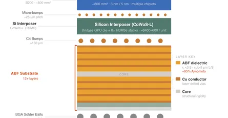
  • **Holistic AI Technology Stack**: The AI buildout extends far beyond GPU silicon to a multi-tiered physical infrastructure stack spanning critical raw minerals, precision semiconductor fabrication, advanced packaging, 800V DC power delivery, and optical interconnects.
  • **Upstream Critical Material Chokepoints**: Essential feedstocks—including Spruce Pine high-purity quartz (HPQ) for Czochralski wafer ingot growth, fluorspar for hydrofluoric acid wet/dry etchants, and byproduct minerals (Indium, Gallium, Germanium, Arsenic)—are subject to severe geopolitical concentration, with China controlling 60–90%+ of global refining.
  • **Advanced Lithography & Patterning Precision**: Transitioning to sub-2nm Gate-All-Around (GAA) nanosheets, 3D NAND (>300 layers), and HBM3e/4 stacks relies on high-aspect-ratio dry plasma etching (Lam, Applied Materials, Tokyo Electron), immersion DUV, High-NA (0.55 NA) EUV machinery, and Metal Oxide Photoresists (MOR).
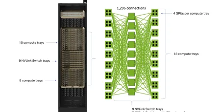
  • **High-Density Power & Thermal Management**: GPU rack power densities scaling past 100 kW drive adoption of 800V DC busbar power delivery, high-reliability polymer/tantalum capacitors for power conditioning, and liquid-cooling pumps driven by NdFeB permanent magnets.
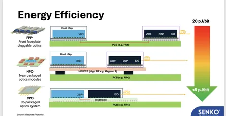
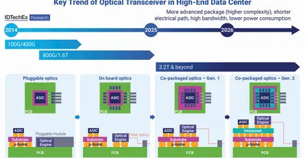
  • **Optical Interconnect & Silicon Photonics Pivot**: Traditional copper interconnects face severe attenuation and thermal limits at 800G/1.6T data center speeds, driving rapid adoption of Indium Phosphide (InP) lasers, GaAs substrates, and Co-Packaged Optics (CPO) to minimize optical transmission energy.
Understanding Semiconductor Etch Machinery: Dry vs. Wet Processes in Advanced Chipmaking

Understanding Semiconductor Etch Machinery: Dry vs. Wet Processes in Advanced Chipmaking

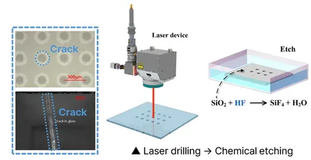
In AI semiconductor fabrication, chipmakers are faced with a monumental challenge: carving out intricate three-dimensional features on a scale measured in angstroms (one ten-billionth of a meter) /sk hynix/. At the heart of this atomic sculpting are two distinct machinery methods: dry plasma etching and wet chemical etching. https://www.youtube.com/watch?v=TWibpFrn45U Plasma etch, dominated by reactive ion etching and inductively coupled plasma systems, acts as the industry's precision laser. By energizing gases into a plasma state, these tools blast ionized particles straight down into a wafer to achieve strict vertical, directional cuts. This capability is non-negotiable for the towering vertical architecture of modern chips, such as 3D NAND memory cells with depth-to-width ratios that exceed one hundred to one /Phys/, or the delicate vertica

read more
How Semiconductor Deposition (CVD, PVD, ALD) Builds AI Silicon

How Semiconductor Deposition (CVD, PVD, ALD) Builds AI Silicon

Semiconductor deposition processes such as Chemical Vapor Deposition (CVD), Physical Vapor Deposition (PVD), and Atomic Layer Deposition (ALD), form the atomic scaffolding of AI chips by layering ultra-pure films that define transistors, interconnects, and three-dimensional memory stacks /Lam Research/. Chemical Vapor Deposition reacts gaseous precursors on a heated wafer to build oxides, nitrides, polysilicon, or tungsten fills at rates of 50–200 nanometers per minute, delivering high uniformity across large surface areas. Physical Vapor Deposition sputters or evaporates atoms from solid targets to create seed layers and metal barriers, such as Titanium Nitride (TiN) and Tantalum Nitride (TaN), prioritizing purity directly from the source material. Atomic Layer Deposition relies on sequential, self-limiting surface reactions to deposit one atomic monolayer per cycle, achieving sub-nanometer thickness control and greater

read more
Inside EUV Lithography: Optics, Power Scaling, and the Physics of Next-Gen Chips

Inside EUV Lithography: Optics, Power Scaling, and the Physics of Next-Gen Chips

Extreme ultraviolet (EUV) lithography systems generate 13.5nm light via laser-produced plasma. A high-power CO₂ laser strikes molten tin droplets up to 50,000 times per second inside a vacuum chamber, creating a plasma that emits the desired photons /TRUMPF/. Both low-NA (numerical aperture of 0.33, resolving ~13nm features) and high-NA (0.55, resolving ~8nm features for denser single-exposure patterning) variants rely on this process. These photons are collected and focused solely by multilayer molybdenum-silicon mirrors (up to 100 alternating bilayers, each a few nanometers thick) polished to atomic-scale smoothness (deviations measured in picometers) with peak reflectivity around 70 percent per surface /Zeiss/. High-NA systems use larger anamorphic optics and half-field scanning to reach ~8nm reso

read more
The Unsung Workhorse: Why DUV Lithography Still Powers the Chip Industry

The Unsung Workhorse: Why DUV Lithography Still Powers the Chip Industry

Deep Ultraviolet (DUV) lithography, primarily using 193nm ArF immersion (ArFi) and 248nm KrF systems, remains essential for patterning the majority of layers in both mature nodes (e.g., 28nm+) and advanced chips /EETimes/. It relies on high-purity photoresists, precise optics, and multi-patterning techniques like self-aligned double/quadruple patterning (SADP/SAQP) to achieve fine features economically. ASML’s TWINSCAN NXT series (e.g., NXT:2050i, NXT:2100i) dominates DUV machinery with throughputs ranging from 4,600 to over 6,300 wafers per day, delivering superior overlay, focus, and productivity for logic, DRAM, and specialty devices.Here is how specific models in the NXT series perform /ASML/:TWINSCAN NXT:1980Fi: Reaches up to 330 wafers per hour (approx. 7,920 theoretically). TWINSCAN NXT:2050i: Produces 295 waf

read more
Nanoimprint Lithography: Patterning the Future of Photonics and Semiconductor Manufacturing

Nanoimprint Lithography: Patterning the Future of Photonics and Semiconductor Manufacturing

In nanoimprint lithography (NIL), a high-precision quartz template (or mold) acts like a stamp, pressing into a low-viscosity resist coated onto a wafer /IEEE/. The resist fills the nanoscale features via capillary action before a standard UV mercury lamp cures the pattern, allowing the template to be cleanly removed. By eliminating the complex optics and high-power light sources required by traditional photolithography, this contact-based approach achieves a 14 nm resolution that is suitable for 5 nm-class logic chips. Beyond standard chips, NIL excels at crafting precise 3D nanostructures ideal for photonics, including waveguides, grating couplers, metasurfaces, and silicon photonic integrated circuits (PICs). Advanced high-index hybrid resists and sol-gel materials further enhance these structures, meeting the strict refractive index and thermal stability demands of modern optical devices. However, several challenges continue to

read more

Frequently Asked Questions

Why is Spruce Pine, NC quartz essential for AI semiconductor manufacturing?

Spruce Pine supplies 70–90% of global high-purity quartz (HPQ) for fused-quartz crucibles used in Czochralski growth of single-crystal silicon ingots at >1,425°C. Ultra-low metallic impurity levels (<50 ppb) are mandatory to prevent crystal defects that ruin yields in advanced sub-2nm AI accelerators.

How do High-NA EUV machinery and metal oxide photoresists (MOR) enable sub-2nm AI accelerators?

ASML High-NA (0.55 NA) EUV systems shrink pitch to sub-10nm without multi-patterning. Pairing High-NA EUV with inorganic Metal Oxide Resists (MOR) offers higher etch selectivity and photon absorption, minimizing line-edge roughness for dense GPU transistor gates.

Why are dry plasma etching and Atomic Layer Deposition (ALD) critical for 3D NAND and GAA nanosheets?

Gate-All-Around (GAA) nanosheets and 3D NAND (>300 layers) rely on dry plasma etching for high-aspect-ratio channel holes with sub-nanometer profile control. ALD then deposits uniform atomic-thin High-k dielectric films (Hafnium oxide) and contact metal liners (Tungsten) into 3D features.

How does optical networking with Indium Phosphide (InP) bypass copper physical limits in AI data centers?

At 800G and 1.6T transceiver speeds, copper interconnects suffer severe thermal dissipation and attenuation. InP-based laser modulators enable Co-Packaged Optics (CPO) and silicon photonics, cutting power per bit and latency across GPU cluster fabrics.

How do 800V DC architectures and NdFeB magnets address 100kW+ GPU rack power densities?

Transitioning server busbars from 48V to 800V DC reduces current by 16x, dramatically lowering copper resistive heat losses. High-coercivity Neodymium-Iron-Boron (NdFeB) magnets drive high-efficiency pumps and fans needed for direct-to-chip liquid cooling.

What supply chain risks affect Indium, Gallium, Germanium, and specialty gases?

Indium, Gallium, and Germanium are byproduct minerals of zinc refining with inelastic supply. With China controlling 60–90%+ of refining and geopolitical concentration in noble gases (Neon, Krypton), supply chokepoints create persistent lead time risks for AI optics and chips.