Why E-Beam Inspection Beats Optical Tools in Sub-5nm Semiconductor Metrology
- David Rogers
- AI Buildout Supply Chain
- 2026-07-29
NEED TO KNOW
- Core Function: E-beam inspection (EBI) and metrology provide sub-nanometer resolution for sub-5nm semiconductor manufacturing where optical light tools fail due to diffraction limits.
- Key Mechanism: Uses voltage contrast (VC) imaging—where grounded structures appear bright and isolated structures appear dark—to pinpoint buried electrical shorts, opens, and leakages in 3D structures like GAA nanosheets and 3D NAND.
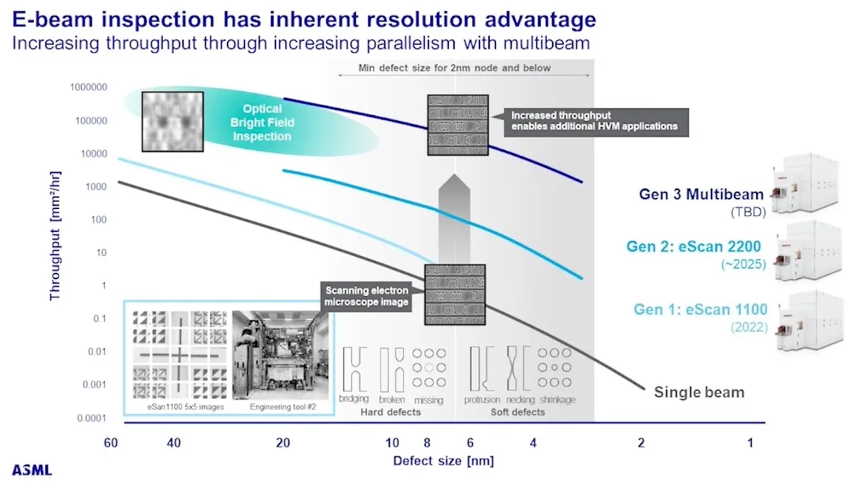
- Throughput Deficit & Mandatory Sub-3nm Adoption: Optical inspection data rates (exceeding 25,000 Mpx/sec) outperform e-beam (~400 Mpx/sec historically) by orders of magnitude. While vendors like Applied Materials, KLA, and ASML are scaling multi-beam architectures and CFE sources to increase throughput, e-beam adoption will accelerate regardless because sub-nanometer resolution and voltage-contrast imaging are mandatory for sub-3nm and GAA nodes.
- Market Leaders: The market is dominated by Hitachi High-Tech (CD-SEM leader), Applied Materials (Cold Field Emission defect review leader), and ASML / HMI (multi-beam eScan pioneer).
Electron semiconductor metrology and e-beam inspection (EBI) are essential tools for modern semiconductor manufacturing /Fabricated Knowledge/. When transistor features drop below 5 nanometers, optical inspection tools cannot resolve them because light diffracts. Focused electron beams provide sub-nanometer resolution to perform inspection where light fails. This high resolution allows engineers to measure complex 3D transistor profiles, evaluate gate dimensions, and inspect line-edge roughness on advanced wafers.
E-Beam Metrology Inspection Process
Automated Wafer Load & Vacuum Pump-Down
Preserving Column IntegrityLoad the 300 mm wafer onto a precision, vibration-isolated stage inside the loadlock module. Transition the atmosphere down to ultra-high vacuum (≤ 10⁻⁷ Pa) to prevent electron scattering by gas molecules and safeguard cathode emission stability.
Electron Gun Initialization & Optics Alignment
Beam Shaping & Aberration CorrectionEmit primary electrons from the cathode (CFE or Schottky TFE) and accelerate them down the column. Precision electromagnetic lenses and MEMS aperture arrays adjust landing energies (typically 100 eV–1 keV) and correct spherical/chromatic aberrations for sub-nanometer beam focusing.
Design-Aware Stage Alignment & Vector Scanning
Hotspot NavigationAlign the wafer using high-precision optical registration. Guided by GDS/OASIS design files, vector-scan high-speed deflection systems drive the primary electron beamlet(s) directly to pre-designated high-risk target sites and 3D hotspots instead of full-die rastering.
Voltage Contrast Induction & Emitted Signal Capture
Defect Surface ChargingIrradiate the surface features to establish dynamic localized charging. Secondary electrons (SEs) and backscattered electrons (BSEs) escape the structure and are filtered by energy analyzers onto high-bandwidth detectors; ungrounded faults trap charge (appearing dark) while grounded lines neutralize (appearing bright).
Real-Time Image Processing & AI Defect Classification
Automated Nuisance FilteringStream raw BSE/SE detector intensity data to high-performance compute nodes. Deep-learning algorithms filter system background noise and instantly classify yield-killing electrical opens, shorts, or bridge defects from benign surface nuances.
EBI systems rely on physics and precision engineering. High-brightness electron sources, such as Schottky field emitters and Cold Field Emission (CFE) sources, emit electrons into ultra-high vacuum columns. Electrostatic and magnetic lenses control the path of these electrons. By setting low electron landing energies, the system can inspect sensitive EUV photoresists without damaging them. EBI uses voltage contrast imaging to detect subsurface faults. Grounded structures allow electric charge to flow and appear bright in images. Isolated structures, electrical open circuits, and leakage paths trap electric charge and appear dark in images.

The primary bottleneck keeping e-beam inspection from replacing optical tools in full-wafer inline scanning has always been throughput speed and data acquisition rates. Historically, optical inspection platforms achieve wafer inspection data rates exceeding 20,000 to 25,000+ megapixels per second, whereas single-beam e-beam inspection operates orders of magnitude slower (typically around 100 to 400 megapixels per second). Because a single electron beam raster-scans a wafer surface line by line, full-die nanometer-scale scanning could take days. To narrow this throughput gap, key semicap suppliers—specifically Applied Materials, KLA (KLAC), and ASML/HMI—are investing heavily in multi-beam MEMS optics arrays (splitting single beams into dozens and eventually thousands of parallel beamlets) alongside high-brightness Cold Field Emission (CFE) sources /ASML/. Combined with AI-driven defect classification and design-aware vector scanning targeting high-risk hotspots, these innovations deliver substantial throughput gains /Applied Materials/. Nevertheless, even with multi-beam scaling, e-beam data rates remain orders of magnitude behind optical inspection. Despite this throughput deficit, e-beam adoption is expanding rapidly because for 3nm, 2nm, and Gate-All-Around (GAA) logic nodes, sub-nanometer physical resolution and voltage-contrast defect detection are mandatory where optical diffraction limits make light-based tools blind.
Driven by the explosive demand for AI hardware, GAA logic nodes, High-NA EUV lithography, and high-layer 3D NAND, the e-beam market is expanding rapidly toward multi-billion-dollar scale. However, supply remains tightly constrained. Building these hyper-specialized vacuum and electron-optic columns isn’t a mass-production affair, and global market share is concentrated among a few key players: Hitachi High-Tech dominates CD-SEM tools, Applied Materials leads in CFE-powered defect review, and ASML pushes multi-beam bounds. As geopolitical export controls tighten, these microscopic tools sit squarely at the center of the global semiconductor push.
Key Insights
What is the estimated install base and tool volume of e-beam inspection and CD-SEM platforms in advanced foundry and memory nodes like TSMC N2, Intel 14A, or SK Hynix 1c/HBM4E?
In leading-edge logic fabs (such as TSMC N2 and Intel 14A) and high-density memory facilities (such as SK Hynix 1c DRAM and HBM4E), yield management represents 15–20% of total fab CapEx, with e-beam process control tools accounting for approximately $12–$15 million per EUV-capable manufacturing line. A standard gigafab module running 40,000 to 50,000 wafer starts per month (WSPM) requires an install base of roughly 30 to 50 automated CD-SEMs (dominated by Hitachi High-Tech’s CG series) alongside 10 to 20 dedicated e-beam defect review and multi-beam inspection systems (such as Applied Materials SEMVision and ASML/HMI eScan) to sustain acceptable yield ramps across Gate-All-Around (GAA) and Backside Power Delivery Network (BSPDN) layers.
What is the most critical process technology bottleneck in scaling multi-beam e-beam inspection (EBI) tools?
The main technical bottleneck in scaling multi-beam EBI tools lies in precision beamlet optics control—specifically, eliminating individual beamlet aberration and electro-optical crosstalk within MEMS micro-lens arrays while maintaining source emission stability. As multi-beam systems scale from 25 beamlets toward thousands (>2,700 beamlets), each micro-column must maintain uniform secondary electron deflection and sub-nanometer spot symmetry without electrostatic coupling or thermal drift between adjacent beams. Furthermore, Cold Field Emission (CFE) tip degradation requires real-time calibration algorithms and localized ultra-high vacuum controls (≤ 10⁻⁹ Pa) to prevent beam current drift across the entire array during high-throughput wafer scans.
What are the unit economics, margin profiles, and supply defensibilities of leading e-beam inspection and metrology equipment?
Advanced e-beam inspection systems feature strong unit economics, with flagship multi-beam and CFE review tools carrying average selling prices (ASPs) between $10 million and $20+ million and generating gross margins of 55% to 65%. The segment shows high defensibility and resilience against semiconductor capital expenditure cycles because chipmakers cannot pause yield defect learning during market downturns without risking technology node delays. Because manufacturing requires ultra-specialized vacuum optics and proprietary electron columns built in low volumes, dominant suppliers (Applied Materials, Hitachi High-Tech, and ASML) secure multi-year Long-Term Supply Agreements (LTSAs) along with high-margin service and software optimization contracts that generate recurring revenue throughout each tool's 10-to-15-year fab lifespan.