AI Buildout & Supply Chain (Page 3)
SiC Power Wafers Powering AI Data Centers: Manufacturing, BPD Challenges & Gen 5 Breakthroughs
- David Rogers
- AI Buildout Supply Chain
- 2026-07-10
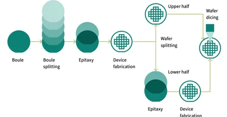
Silicon carbide (SiC) power wafers are the critical enabler for the next wave of AI infrastructure. Hyperscale data centers running dense GPU clusters consume staggering amounts of electricity; traditional silicon power devices simply cannot deliver the efficiency, power density, and thermal performance required. SiC MOSFETs and diodes cut switching and conduction losses dramatically (often 50%+ vs. silicon), support higher bus voltages for slimmer distribution architectures, and reduce cooling overhead—directly addressing the power wall facing AI buildouts by hyperscalers /HIITIO/. The same technology is already transforming 800V electric vehicle drivetrains and renewable inverters, but AI data-center power supplies are now emerging as a powerful new growth vector /NVIDIA/. https
read moreSOI Wafers: The Critical Substrate Powering Silicon Photonics for AI Data Centers
- David Rogers
- AI Buildout Supply Chain
- 2026-07-09
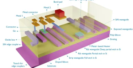
Silicon-on-insulator (SOI) wafers are the foundational engineered substrate enabling high-performance silicon photonics (SiPh) platforms critical to AI data center scaling. These wafers feature a thin single-crystal silicon device layer atop a buried oxide (BOX) insulating layer on a silicon handle wafer. For SiPh applications, typical specs include a precisely controlled top silicon layer (often ~220–300 nm) and a thicker BOX (commonly 2–3 μm) that provides excellent optical confinement, low propagation loss in waveguides, and electrical isolation /UniversityWafer/. This structure supports monolithic or heterogeneous integration of passive photonic components (waveguides, modulators, mux/demux) alongside electronics, delivering the ultra-high bandwidth, low latency, and energy efficiency needed for optical interconnects replacing copper in hyperscale AI clusters. https://www.youtube.com/watch?v=T-prNhiLLZ8 Produ
read more300mm Silicon Wafers: The Precision Foundation Powering AI Chip Production
- David Rogers
- AI Buildout Supply Chain
- 2026-07-08
Every advanced AI accelerator, GPU, and high-bandwidth memory chip begins life on a 300mm silicon wafer, a near-atomically flat, defect-free single-crystal disk /NIST/. Production starts with abundant quartz sand reduced to metallurgical-grade silicon, then purified to electronic-grade polysilicon (typically 9N–12N purity, or 99.9999999%+). Specialists like Wacker Chemie (Europe’s leader in hyperpure semiconductor-grade polysilicon) supply this feedstock /Wacker/. It is melted in a quartz crucible at ~1,414 °C inside a Czochralski (CZ) puller; a seed crystal is dipped, rotated, and slowly withdrawn to grow a massive dislocation-free boule. The ingot is cropped, ground, diamond-wire sliced, edge-profiled, lapped, etched, and chem-mechanically polished to nanometer flatness and sub-parts-per-billion metallic
read more
Fluorspar: The Critical Mineral Powering Precision Etching in AI Semiconductors
- David Rogers
- AI Buildout Supply Chain
- 2026-07-07
Fluorspar (fluorite, CaF₂) is the primary global source of fluorine and the essential feedstock for hydrofluoric acid (HF). In advanced semiconductor fabrication, HF enables the precise wet etching of silicon dioxide layers and ultra-cleaning of silicon wafers /Kern/. These processes define the nanoscale features in logic chips, memory, and advanced packaging critical to AI accelerators and high-performance computing. No economical substitute matches HF’s selectivity and atomic-level control for sub-5nm and future nodes; without reliable HF supply, AI chip production scales would stall. Acid-grade fluorspar (≥97% CaF₂) reacts with concentrated sulfuric acid in rotary kilns or furnaces at 200–300°C to produce HF gas (CaF₂ + H₂SO₄ → 2HF + CaSO₄), which is then condensed and distilled. Semiconductor-grade “ultra-high-purity” (UHP) HF demands additional multi-stage purification to achieve parts-per-billion impurity levels, especially removing ar
read more
Arsenic: The Toxic Critical Mineral Powering GaAs Semiconductors for AI
- David Rogers
- AI Buildout Supply Chain
- 2026-07-06
Arsenic is the critical and highly problematic feedstock that makes gallium arsenide (GaAs) compound semiconductors possible. GaAs excel where silicon hits physical limits: superior electron mobility and direct bandgap enable high-frequency RF/power amplifiers (critical for 5G/6G base stations and wireless edge AI), optoelectronic devices (Vertical-Cavity Surface-Emitting Laser or VCSEL), and specialized photonics or defense-grade chips. In AI infrastructure, GaAs VCSEL arrays support energy-efficient optical interconnects in data centers /Chalmers/ that reduce power and latency for massive AI training/inference clusters while RF components enable low-latency wireless backhaul and distributed intelligence. Producing electronic-grade GaAs demands extreme purity and specialized handling /LibreText/06%3A_Gro
read more