X-Ray Semiconductor Metrology: Principles, Market Growth, and Key Players
- David Rogers
- AI Buildout Supply Chain
- 2026-07-30
NEED TO KNOW
- Capabilities & Techniques: X-ray metrology provides non-destructive, subsurface 3D inspection beyond optical and e-beam limits. Key methods include CD-SAXS (nanoscale profiles), HRXRD (strain/defects), XRR (film thickness/density), TXRF (contamination), and CT (package voids).
- Hardware Innovations: Bright liquid-metal-jet anodes offer up to 27× higher brightness over solid anodes, while AI inverse modeling and hybrid metrology reduce data analysis times from hours to seconds.
- Technical Bottlenecks: Primary manufacturing hurdles include throughput constraints (low flux), radiation damage to HBM dielectrics, low material contrast in 2.5D/3D packages, and noisy scatterometry reconstruction.
- Market Trajectory: Driven by GAA nanosheets, 3D NAND, and AI packaging, the semiconductor X-ray metrology market is projected to reach ~$3.5B by 2032 (~13% CAGR).
- Industry Supply Chain: Top suppliers include Bruker, Rigaku, Malvern Panalytical, Sigray, Nordson, Comet Yxlon, and Nikon Metrology. Production remains concentrated in the US, Europe, and Japan.
X-ray semiconductor metrology and inspection provides non-destructive, subsurface, and three-dimensional views of high-aspect-ratio (HAR) and buried structures. Optical and electron-beam tools cannot fully inspect these deep features. Specialized techniques measure key physical properties across different semiconductor layers:
- High-Resolution X-ray Diffraction (HRXRD): Measures crystallographic strain, lattice defects, and material phase.
- X-ray Reflectivity (XRR): Measures thin-film thickness, layer density, and surface roughness.
- X-ray Fluorescence (XRF/TXRF): Identifies elemental composition and trace metal contamination.
- Critical-Dimension Small-Angle X-ray Scattering (CD-SAXS): Measures nanoscale shape profiles, sidewall angles, and critical dimensions.
- X-ray Computed Tomography (CT): Detects internal voids, micro-cracks, and interconnect failures in 3D structures.
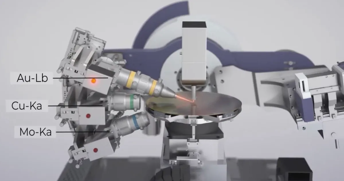
These methods use specialized equipment to generate and capture X-rays. Systems pair sensitive detectors with computational reconstruction software to convert raw signals into structural models. Conventional X-ray tools use solid metal anodes, but high beam power can melt these targets and limit total light brightness. Newer liquid-metal-jet sources use a stream of molten metal alloy to remove heat rapidly. This design increases source brightness by roughly an order of magnitude. As a result, laboratory instruments can now perform high-precision measurements that previously required large synchrotron facilities. At the same time, artificial intelligence (AI) and hybrid metrology—which combine X-ray data with optical or electron-beam results—reduce data processing times from hours to seconds.
CD-SAXS Metrology & Structural Reconstruction Process
Wafer Loading & Precise Target Alignment
Sub-Micron Stage PositioningLoad the silicon wafer onto a high-precision, vibration-isolated stage and align the high-aspect-ratio measurement target directly with the X-ray beam path.
High-Brightness X-Ray Generation & Optics Focusing
Beam ConditioningGenerate a focused hard X-ray beam using a liquid-metal-jet anode source, passing it through specialized capillary optics to achieve sub-nanometer wavelength collimation.
Multi-Angle Transmission & Scattering Data Collection
Angle-Resolved MeasurementPass the hard X-ray beam completely through the wafer target while tilting the stage across multiple incident angles, recording reciprocal-space elastic scattering patterns on a photon-counting detector.
AI-Accelerated Inverse Modeling & Profile Reconstruction
Structural Parameter ExtractionProcess the raw 2D diffraction intensity maps through deep neural networks and inverse scatterometry solvers to reconstruct 3D nanoscale parameters, such as pitch walking, sidewall angles, and critical dimensions.
Engineers face four primary technical challenges when deploying X-ray systems directly into high-volume manufacturing: limited throughput due to low X-ray flux on fast logic production lines, radiation damage where high-energy rays trap electrical charges in sensitive layers like High-Bandwidth Memory (HBM) dielectrics, low material contrast between similar-density materials in 2.5D/3D packages, and the high computational complexity of reconstructing images from sparse or noisy scattering data. To overcome these hurdles, industry developers are building brighter compact sources and using deep neural networks (such as ResNet regression models) to reconstruct complete structural profiles from significantly fewer measurement angles. Additionally, designers employ layout-aware AI to direct inspection exclusively to high-risk features on the wafer, dramatically reducing overall scan times and processing overhead.
To solve these issues, industry developers are building brighter compact sources and using deep neural networks (such as ResNet regression models) to reconstruct full images from fewer measurement angles. Designers also use layout-aware AI to focus inspection specifically on high-risk features on the wafer.
Demand for X-ray metrology is growing as chipmakers adopt complex transistor designs and dense memory architectures. Key drivers include gate-all-around (GAA) nanosheets, forksheets, complementary FETs (CFETs), ultra-high-aspect-ratio 3D NAND flash, HBM stacks, and heterogeneous 2.5D/3D packaging for AI accelerators. Market analysts estimate X-ray defect-inspection systems are growing at 6% to 8% annually /Mordor Intelligence/, driven by advanced packaging quality control.
| Supplier | Primary Product Focus | Application Range |
|---|---|---|
| Bruker | XRD, XRR, TXRF, CD-SAXS | Front-end wafer metrology & research |
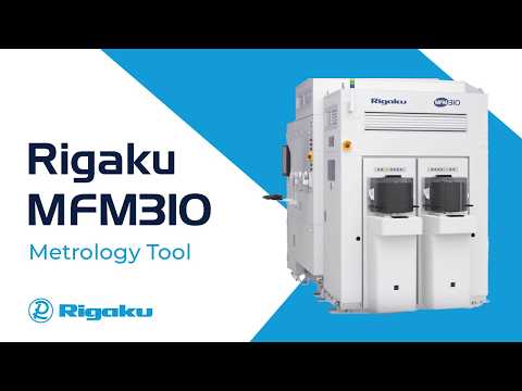
| Rigaku | Inline CD-SAXS, HRXRD, XRR | High-volume wafer manufacturing |
| Malvern Panalytical | High-resolution XRD & XRR | Thin-film & materials characterization |
| Sigray | Micro-XRF & sub-micron CT | High-brightness lab-to-fab inspection |
| Nordson Test & Inspection | Automated X-ray Inspection (AXI) | Advanced packaging & board assembly |
| Comet Yxlon | Microfocus & nanofocus CT | Subsurface void & joint inspection |
| Nikon Metrology | High-resolution X-ray CT | Packaging & structural inspection |
A small number of specialized vendors in the United States, Japan, and Europe control the production of high-performance components, including X-ray optics, liquid-jet sources, and photon-counting detectors. While Chinese manufacturers produce standard packaging and circuit-board inspection tools, they rely on Western and Japanese suppliers for leading-edge metrology. Consequently, trade controls and supply-chain restrictions present strategic risks for advanced wafer fabs and global AI hardware production.
Key Insights
What is the estimated tool install base for X-ray metrology in advanced semiconductor nodes like TSMC N2, Intel 14A, and SK Hynix 1c/HBM4E?
At leading-edge logic nodes such as TSMC N2 and Intel 14A, high-throughput inline and near-fab X-ray metrology tools (specifically CD-SAXS and HRXRD) are deployed at a density of roughly 4 to 8 tools per 50,000 wafer-starts-per-month (WSPM) gigafab line, primarily stationed at gate-all-around (GAA) nanosheet etch and epitaxy clusters. In advanced memory production, such as SK Hynix 1c DRAM and HBM4E multi-die stacks, high-aspect-ratio (HAR) channel hole profile measurement and microbump interconnect verification require an estimated 6 to 10 X-ray inspection and metrology units per 50k WSPM. Across a multi-billion-dollar fab module, this translates to an initial capital expenditure of $30M to $70M dedicated exclusively to X-ray diagnostic hardware, with total industry fab shipments expanding as 3D scaling moves beyond the physical penetration limits of conventional optical and e-beam tools.
What is the most critical bottleneck process technology where X-ray metrology is strictly indispensable?
The single most critical process bottleneck requiring X-ray metrology is full-depth 3D profile reconstruction in sub-2 nm Gate-All-Around (GAA) nanosheets and Ultra-High-Aspect-Ratio (UHAR) 3D NAND structures (>200–300 layers). In these deep features, traditional optical scatterometry suffers from severe light opacity and multi-reflection distortion, while CD-SEM e-beams cannot penetrate beyond the top few nanometers without damaging sensitive oxide layers. Critical-Dimension Small-Angle X-ray Scattering (CD-SAXS) is the only non-destructive technique capable of probing sub-nanometer sidewall angles, pitch walking, inner spacer geometry, and channel-hole tilt down through multi-micron-deep structures. Without continuous inline CD-SAXS monitoring, minor deviations in plasma etch tilt or sacrificial layer thickness propagate undetected into catastrophic yield loss and electrical shorting across 3D device stacks.
What are the unit economics, gross margins, and cyclicality of semiconductor X-ray metrology systems?
Semiconductor X-ray metrology tools command high Average Selling Prices (ASPs) ranging from $3.5 million for standalone lab-to-fab XRR/XRD systems to over $8 million to $12 million for advanced inline CD-SAXS and high-resolution automated X-ray CT clusters. Tier-1 equipment vendors enjoy gross margins of 50% to 60%+ due to high intellectual property barriers around specialized components—such as proprietary liquid-metal-jet anodes, precision capillary optics, and photon-counting detector arrays. Fabs typically acquire these systems through multi-year Long-Term Supply Agreements (LTSAs) bundled with high-margin annual software licenses and calibration servicing (accounting for 15–20% of recurring tool revenue). While front-end wafer equipment expenditure remains tied to general semiconductor capital cycles, X-ray metrology exhibits higher margin defensibility than general metrology due to structural tailwinds from non-optional 3D transitions (GAA, HBM4, advanced packaging) that demand increased metrology intensity per wafer node transition.