Silicon Photonics Foundries: Manufacturing, Scaling, and Market Outlook
- David Rogers
- AI Buildout Supply Chain
- 2026-08-03
NEED TO KNOW
- Silicon photonics foundries manufacture Photonic Integrated Circuits (PICs) by building optical components on Silicon-on-Insulator (SOI) substrates using standard 200 mm and 300 mm CMOS semiconductor equipment.
- Because silicon has an indirect bandgap that prevents efficient light emission, foundries hybrid-integrate external III-V direct-bandgap lasers (such as Indium Phosphide) onto the silicon die via molecular bonding or photonic wire bonding.
- Explosive bandwidth demand from AI GPU clusters and hyperscale data centers is driving the silicon photonics market from $2–3B (2024–2025) toward $9–15B by 2030–2035 at a 25–30% CAGR.
- GlobalFoundries (following its late-2025 acquisition of Singapore’s AMF) and Tower Semiconductor lead pure-play capacity, alongside major integrated players including TSMC (COUPE platform), STMicroelectronics, and Intel.
- Key industry challenges include sub-micron alignment tolerances for Co-Packaged Optics (CPO), thermal expansion mismatches in hybrid lasers, limited 300 mm photonics-qualified PDKs, and complex heterogeneous material recycling.
Silicon photonics foundries manufacture photonic integrated circuits (PICs) on silicon-on-insulator (SOI) wafers using CMOS-compatible processes /PhotonDelta/. Combining CMOS manufacturing scale with optical features lets companies build dense, low-power optical interconnects at a fraction of the cost of pure III-V photonics.
Silicon Photonics Foundry Process Breakdown
SOI Substrate Preparation
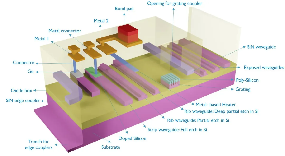
Establishing the Base Waveguide CoreStart with a Silicon-on-Insulator (SOI) wafer featuring a thin monocrystalline silicon device layer atop a buried oxide (BOX) layer to ensure optical confinement.
Deep-UV Lithography
Patterning Sub-Micron FeaturesApply deep-ultraviolet (DUV) lithography (193 nm or immersion) to define narrow waveguide paths, rib structures, and grating couplers across the wafer.
Precision Dry Etching
Forming Low-Loss Waveguide SidewallsPerform reactive-ion etching (RIE) to carve silicon waveguides, maintaining sidewall roughness near ~1 nm to minimize optical propagation loss.
Doping & Implantation
Creating Electro-Optic Modulator JunctionsIon-implant boron and phosphorus to form p-n/p-i-n junctions in silicon, enabling fast optical phase modulation via free-carrier dispersion.
Germanium Epitaxy
Integrating On-Chip PhotodetectorsSelectively grow Germanium (Ge) via chemical vapor deposition in designated cavities to build high-responsivity photodiode detectors for 1310/1550 nm wavelengths.
Dielectric Deposition & Cladding
Insulating & Passivating the Photonic LayerDeposit thick silicon dioxide (SiO₂) top cladding to isolate optical modes from metal interconnects and protect passive components from environmental damage.
III-V Laser Hybrid Integration
Adding On-Chip Light SourcesAttach or die-bond Indium Phosphide (InP) gain blocks onto the silicon substrate using molecular direct bonding or micro-transfer printing to supply optical power.
Back-End-of-Line (BEOL) Metallization
Routing Electrical Contacts & HeatersDeposit aluminum or copper interconnect layers and titanium micro-heaters to supply electrical drives for modulators and thermal phase shifters.
Facet Preparation & Optical Fiber Coupling
Enabling Chip-to-World Optical I/OEtch deep V-grooves or polish chip edge couplers, then align and bond optical fibers or photonic wire bonds for sub-micron light transfer.
Wafer-Level Testing & Dicing
Quality Assurance & Final SingulationExecute automated wafer-scale electro-optical probing to test spectral response and optical power before dicing wafers into individual PIC dies.
Key challenges center on light generation, packaging, and high-volume yield. Integrating hybrid lasers remains difficult because of thermal expansion differences, tight alignment tolerances, and potential yield loss /GF/. Connecting optical fibers or free-space optics to the chip, especially in co-packaged optics (CPO), requires sub-micron placement precision and drives up packaging costs. Emerging solutions include direct wafer bonding, photonic wire bonding, detachable fiber mounts, and advanced packaging facilities located next to fabs. Fabs are also moving production from 200mm to 300mm wafers with mature process design kits (PDKs). These improvements aim to lower costs, raise manufacturing yields, and reduce production cycles as data rates reach 200–400G per wavelength /TrendForce/.
Demand is growing rapidly due to AI and hyperscale data centers. Silicon photonics provides the high-bandwidth, low-power, and low-latency optical interconnects needed for GPU clusters and high-speed network switches operating at 800G and above. The total silicon photonics market was worth roughly $2–3 billion in 2024–2025 and is projected to reach $9–15 billion by 2030–2035 (growing at 25–30% annually) /Mordor Intelligence/. Data center and high-performance computing (HPC) networks are the main growth drivers, and optical transceiver manufacturing is shifting heavily toward silicon-photonics modulators. Secondary markets include telecommunications, LiDAR, environmental sensing, optical computing, and quantum systems.
Specialized foundry capacity is expanding quickly, but demand still outpaces supply. GlobalFoundries and Tower Semiconductor are the clearest capacity leaders in the market. GlobalFoundries holds a leading pure-play position after acquiring Singapore’s Advanced Micro Foundry (AMF) in late 2025; it operates 300 mm lines in Malta, New York, and plans to upgrade AMF to 300mm capability. Tower Semiconductor operates fabs across the US, Israel, and Japan, expanding its 300 mm capacity through major customer contracts and Japanese government support /Tower/. Other key suppliers include Intel with proprietary manufacturing lines, STMicroelectronics with high-volume 300mm production, TSMC with its COUPE platform for CPO integration /Tom’s Hardware/, and smaller fabs like Silterra supplying 200mm wafers. Raw silicon and basic SOI wafers are readily available, but 300mm photonics capacity, certified PDKs, and external III-V lasers remain supply bottlenecks. Additionally, recycling finished photonic chips is still difficult because they contain a mix of different materials.
Geopolitically, the supply base is geographically spread out, but key dependencies remain. Major production facilities operate in the United States (GlobalFoundries), Singapore (AMF/GF), Japan and Israel (Tower), Taiwan (TSMC), Europe (STMicroelectronics and IMEC), and Malaysia. This global spread reduces single-point risks compared to logic chip production. However, concentration risks persist due to high reliance on Taiwan, strict US-China export controls on advanced packaging, and limited suppliers for specialized SOI wafers and III-V lasers. Government incentives, such as US CHIPS Act funding and national capacity projects in Japan and Europe, directly target these risks to build resilient supply chains for AI infrastructure.
Key Insights
How are silicon photonics foundries and AI accelerator architectures (e.g., NVIDIA Vera Rubin, AMD Helios) scaling optical volume?
Specialized pure-play and hybrid foundries—led by GlobalFoundries, Tower Semiconductor, and TSMC (via its COUPE platform)—are rapidly scaling 300 mm wafer capacity to support millions of optical engines required by next-generation AI clusters. In architectures like the NVIDIA Vera Rubin platform (utilizing Spectrum-X Ethernet Photonics) and AMD Helios rackscale systems, traditional copper scale-out connections hit strict thermal and reach limits at 200G–400G per lane. These platforms integrate silicon photonics directly into co-packaged optics (CPO) and near-packaged optics (NPO) switch engines to drive hundreds of terabits per second of rack-to-rack interconnect. This shift is expanding silicon photonics from a niche transceiver market into high-volume semiconductor fabrication, with CPO/NPO optical engines projected to reach a $39 billion market opportunity by 2030.
What is the most critical process bottleneck in silicon photonics manufacturing?
The most critical process technology bottleneck in high-volume silicon photonics is sub-micron optical coupling and heterogeneous III-V laser integration. Because silicon’s indirect bandgap prevents efficient native light generation, foundries must integrate external gain mediums—typically Indium Phosphide (InP) or Gallium Arsenide (GaAs) lasers—onto silicon substrates. Achieving reliable hybrid bonding or photonic wire bonding with placement accuracy under ±0.5 µm while managing thermal expansion mismatches (CTE of InP vs. Si) creates severe yield loss and drives up back-end packaging costs, which currently account for 50% to 80% of total module expenses.
How do unit economics, long-term supply agreements, and margin defensibility shape the silicon photonics market?
Silicon photonics unit economics benefit from high gross margins and strong defensibility due to steep technological barriers, proprietary Process Design Kits (PDKs), and high switching costs once a design is qualified on a specific 300 mm line. Unlike traditional cyclical commodity memory or standard logic, market growth is secured through multi-year Long-Term Supply Agreements (LTSAs) between hyperscalers/chipmakers and foundries (such as Tower and GlobalFoundries) to guarantee 300 mm capacity and continuous Continuous Wave (CW) laser supply. As module assembly transitions from labor-intensive manual optical alignment to automated CMOS-style wafer-level packaging, manufacturing yields rise, expanding gross margins and shielding leading pure-play foundries from typical semiconductor downcycles.