Compound Semiconductors Explained: GaN, SiC, and InP in the AI & EV Era
- David Rogers
- AI Buildout Supply Chain
- 2026-08-05
NEED TO KNOW
- Core Materials & Roles: SiC powers high-voltage EV inverters (800 V), GaN drives high-frequency AI data center power delivery, and InP enables 800G/1.6T optical interconnect lasers.
- Scaling Dynamics: The industry is transitioning to 200 mm (8-inch) SiC and 150 mm (6-inch) InP wafers to reduce die costs by 50%–60% and raise production throughput.
- Manufacturing Challenges: Production yields are highly sensitive to defect densities (micropipes, basal-plane dislocations, and threading defects) and slow crystal growth rates (PVT for SiC).
- Supply Chain Risks: Gallium and indium are by-products of aluminum and zinc refining; dominant refined supply in China and export controls make primary supply security and recycling strategic priorities.
Compound semiconductor foundries for GaN, SiC, and InP sit at the heart of the AI, EV, and high-frequency electronics buildout. They turn wide-bandgap materials into power devices, RF amplifiers, and photonic chips that silicon cannot match. Foudries grow and process InP crystals into substrates for lasers and detectors. All demand high purity and low defect densities (micropipes, basal-plane dislocations, threading defects) to support high-voltage, high-frequency, or high-optical-performance devices. These requirements make production yields far more sensitive than conventional silicon yields /PhotonDelta/.

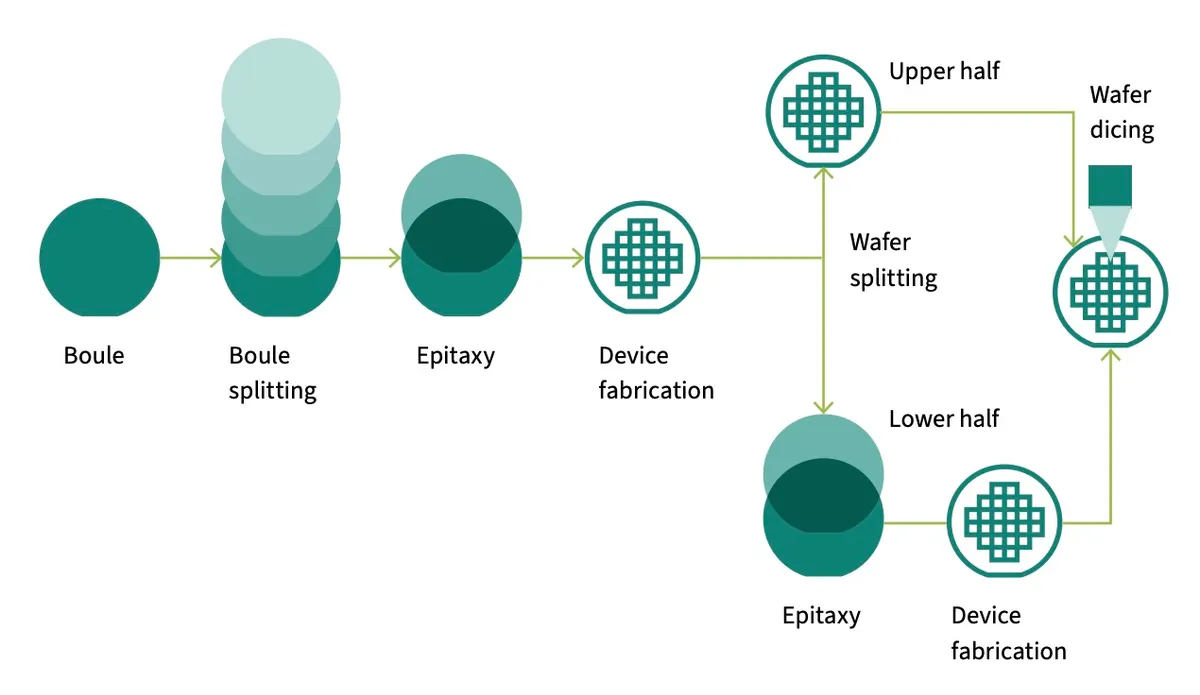
The main technical challenges remain crystal quality at larger diameters, slow growth rates for SiC boules, and epitaxial uniformity. Companies race to 200 mm (8-inch) SiC wafers and 150 mm (6-inch) InP wafers to cut die costs by 50 to 60 percent and raise output. Wolfspeed’s Mohawk Valley fab, Infineon’s Kulim Module 3 /Infineon/, STMicroelectronics’ Catania integrated substrate line /ST/, and Coherent’s Sherman and Järfälla 6-inch InP lines show this shift clearly. Parallel efforts target lower defect densities, recycled precursor gases, and hybrid integration (GaN-on-Si, InP-on-Si) to reduce waste and cycle time.
Demand is growing rapidly as SiC and GaN power devices serve EV inverters, onboard chargers, solar arrays, industrial drives, and AI data-center power delivery (800 V architectures). InP supplies the electro-absorption modulated lasers, continuous-wave sources, and photonic integrated circuits required for 800G/1.6T optical links inside those same data centers, plus 5G/6G RF and sensing systems. Market forecasts show SiC and GaN power segments growing at 15 to 30 percent CAGRs through the early 2030s /Mordor Intelligence/, with InP wafer and device demand tied directly to hyperscale AI interconnect build-outs.
Production capacity remains tight relative to projected needs. SiC substrate and device capacity expands rapidly in the US, Europe, Japan, and China (Wolfspeed, Infineon, ST, onsemi, ROHM, SICC, Sanan). Meanwhile, IDMs and foundries like Qorvo, Navitas, Innoscience, and MACOM share GaN manufacturing. InP remains more concentrated, with Coherent leading the move to high-volume 6-inch production while receiving CHIPS Act support /Coherent/.
Key Insights
How are compound semiconductors deployed in next-generation AI accelerator architectures like NVIDIA Vera Rubin NVL72 or AMD Helios, and what are their estimated install volumes per rack scale?
In ultra-dense rack architectures like NVIDIA’s Vera Rubin NVL72 and AMD Helios, compound semiconductors fulfill specialized roles in optical interconnects and power delivery where silicon cannot operate. Indium Phosphide (InP) is the critical component for high-speed optics, providing the direct bandgap substrate for the Electro-absorption Modulated Lasers (EMLs) and Continuous-Wave (CW) light sources inside scale-out optical transceivers and co-packaged optical (CPO) engines. A single Vera Rubin NVL72 or AMD Helios rack deploying 1.6T optical links utilizes an estimated 144 to 288 InP laser channels across its SuperNICs and switch trays to support up to 260 TB/s of scale-up and scale-out fabric bandwidth. Concurrently, Gallium Nitride (GaN) and Silicon Carbide (SiC) power devices populate the rack power shelf—converting high-voltage AC mains down to 800 V and 48 V DC—with a single 160–170 kW rack requiring several hundred discrete GaN/SiC power switches to achieve >98% power delivery efficiency under extreme computing loads.
What are the primary crystal growth and manufacturing bottlenecks limiting SiC and InP wafer yield at 150 mm and 200 mm diameters?
While silicon foundries scaling advanced nodes (such as TSMC N2 and Intel 14A) face High-NA EUV lithography constraints, compound semiconductor foundries are bottlenecked by bulk crystal growth kinetics and defect mitigation during epitaxy. For SiC, the primary constraint is physical vapor transport (PVT) growth, which operates at ultra-slow rates (0.1–0.5 mm/hr) and generates high densities of Basal Plane Dislocations (BPDs) and micropipes that degrade high-voltage yield. For InP integrated with high-volume Si memory or compute nodes (such as SK Hynix 1c DRAM and HBM4E stack interfaces), the critical bottleneck is managing the thermal expansion coefficient (CTE) and lattice mismatch during heteroepitaxy or direct wafer bonding. Mitigating thread dislocation propagation without causing thermal stress-induced cracking limits substrate yields and requires complex buffer layer deposition, directly constraining the availability of 150 mm InP and 200 mm SiC wafers across compound foundries.
What are the unit economics, margin growth drivers, and supply risks governing compound semiconductor substrate manufacturing?
Compound semiconductor unit economics are characterized by high gross margin defensibility (45%–55%+ for leading substrate suppliers) paired with structural supply risks and capital intensity. Margin expansion is primarily driven by the yield-improving transition from 150 mm (6-inch) to 200 mm (8-inch) substrates, which increases die-per-wafer yields by ~78% and slashes nominal per-die manufacturing costs by 50%–60%. To insulate against semiconductor cyclicality, foundries enter multi-year Long-Term Supply Agreements (LTAs) with key IDMs and hyperscalers, securing baseline utilization for high-CAPEX facilities like Wolfspeed’s Mohawk Valley or Infineon’s Kulim Module 3. However, long-term unit economics remain vulnerable to geopolitical bottlenecks; because primary gallium and indium are by-products of aluminum and zinc smelting predominantly refined in China, export restrictions on raw metals force reliance on high-cost primary refining or circular scrap recycling, creating input price volatility for device makers.
What is the planned future foundry capacity expansion for compound semiconductors across major global manufacturing regions?
Global compound semiconductor foundry capacity is undergoing a massive multi-billion-dollar expansion through 2030, driven by sovereign subsidies (such as the U.S. and European CHIPS Acts) and a synchronized transition to 200 mm (8-inch) wafer lines. In Europe, Infineon’s Kulim Module 3 expansion in Malaysia along with STMicroelectronics’ integrated Catania campus in Italy are targeting a combined multi-gigawatt power output, with Infineon alone aiming to capture 30% of the global SiC market by 2030. In North America, Wolfspeed’s 200 mm Mohawk Valley and Siler City expansions alongside Coherent’s CHIPS Act-supported Sherman InP fab expansion lead domestic capacity growth. Meanwhile, Asia-Pacific remains the highest-volume production hub; China is building out significant domestic capacity—projected at over 8 million wafers per month across SiC/GaN processing nodes (via Sanan IC, SICC, and local foundries)—while pure-play foundries like TSMC are expanding dedicated GaN-on-Silicon lines to support global fabless power and RF customers.