Inside Compound Semiconductor MOCVD: Technology, Markets, and Supply Chain Constraints
- David Rogers
- AI Buildout Supply Chain
- 2026-08-04
NEED TO KNOW
- Core Technology: Metal-Organic Chemical Vapor Deposition (MOCVD) is the dominant industrial method for growing high-purity compound semiconductor crystals (GaN, InP) on substrates like silicon, sapphire, and SiC.
- Primary Applications: GaN powers high-efficiency power electronics, EV chargers, 5G/6G RF, and microLEDs. InP underpins optical communications (lasers, modulators, detectors) critical for AI data center interconnects.
- Key Challenges: Growth performance is limited by lattice mismatch defects, wafer bow on larger diameters (up to 200 mm), low precursor utilization, and handling hazardous gases (NH₃, PH₃).
- Equipment Landscape: Aixtron and Veeco command the majority of global MOCVD tool supply (~55–75% historically), with Chinese vendors (AMEC, NAURA) expanding market share in volume LED and power sectors.
- Supply & Geopolitical Bottlenecks: Growth is constrained by tool lead times and single-crystal substrate manufacturing (led by Japan for InP), driving regional subsidies (US/EU CHIPS Acts) and export controls.
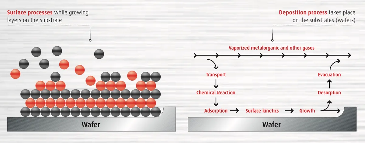
Compound semiconductor epitaxial growth using MOCVD (metal-organic chemical vapor deposition) is the main industrial method for depositing high-quality crystal layers of materials like GaN (gallium nitride) and InP (indium phosphide) /Aixtron/. Hydrogen gas carries high-purity organometallic chemicals (trimethylgallium, trimethylindium) and hydrides (ammonia, phosphine) into a heated reactor. These gases break down on base materials called substrates (sapphire, silicon, silicon carbide, or native wafers) to form precisely controlled layer stacks, quantum wells, and doped regions. Ultra-high chemical purity (99.9999% to 99.99999%+) is critical: even tiny traces of oxygen, carbon, or metal contamination create defects that reduce laser efficiency, transistor mobility, or LED performance. MOCVD’s main advantage is its ability to grow complex, multi-layer wafer stacks across many wafers at once with high output, making it better suited for volume production than molecular-beam epitaxy.
Key technical challenges include mismatch in crystal structure and thermal expansion (especially when growing GaN on silicon or sapphire), which creates high defect density in the material. Other challenges include maintaining uniform thickness and chemical mix across larger wafers (moving to 150–200 mm InP and 200 mm GaN-on-silicon), waste of input gases caused by high supply ratios and high heat, and handling toxic, self-igniting gases. Emerging efforts to reduce cost, waste, and processing time focus on advanced gas-flow reactor designs (planetary and showerhead systems), in-situ chamber cleaning, chemicals that break down at lower temperatures, GaN-on-silicon integration for silicon-foundry compatibility /GF/, hydride vapor-phase epitaxy for fast growth of thick base layers, and improved chemical recycling.

End markets are growing quickly. GaN is used in power electronics (EV chargers, data-center power supplies, radio-frequency chips for 5G/6G) and lighting/microLED displays. InP supports optical devices such as lasers, modulators, and light detectors for telecommunications and AI data-center optical connections (such as electro-absorption lasers and high-power continuous-wave lasers for co-packaged optics). Demand for InP optics has grown so fast that supply limits are affecting production /Tom’s Hardware/, with large data-center operators needing hundreds of millions of units and market forecasts projecting multi-billion-dollar laser sales by 2030. Overall, the markets for compound semiconductor substrates and processed wafers are projected to grow at strong annual rates through the early 2030s /Yole/.
Production capacity is limited by equipment availability and raw crystal substrate manufacturing, rather than raw mineral reserves in the earth. Aixtron (Germany) and Veeco (US) supply most of the MOCVD equipment market (historically 55–75% combined, with Aixtron leading in InP and advanced GaN systems); Chinese vendors like AMEC and NAURA are gaining market share in high-volume LED and power applications. Major substrate and processed-wafer suppliers include IQE, Sumitomo Electric, AXT, and Coherent. Refineries collect gallium and indium mainly as secondary by-products during aluminum and zinc processing /EI/; scrap wafer recycling recovers additional indium and gallium, though recycled amounts remain small compared to primary refining.
Geopolitical concentration creates real supply risks. Japanese manufacturers have long led the market for high-quality InP substrates; China holds a large portion of installed MOCVD machine capacity and LED production while working to produce its own tools and raw materials locally. The United States and Europe are using government funding programs to build domestic production capacity for power and optical chips, while export rules restrict the flow of advanced manufacturing tools. Proposed U.S. import bans targeting Chinese data center hardware and optical transceivers threaten to intensify these risks, shifting more demand to non-Chinese suppliers and tightening western wafer-capacity bottlenecks /Reuters/. Strong demand for InP optical chips is highlighting these manufacturing limits, making reliable layer-growth capacity a key priority for expanding semiconductor and data-center systems.
Key Insights
What are the estimated volume requirements for InP optical components in leading AI accelerator platforms like NVIDIA Vera Rubin or AMD Helios?
Next-generation AI accelerator systems, such as the NVIDIA Vera Rubin platform and AMD Helios rack-scale architectures, rely heavily on 1.6T optical interconnects (8×200G per lane) to handle scale-out traffic across massive AI factory clusters. While intra-rack domain connections often utilize direct-attach copper, inter-rack scale-out links demand Electro-absorption Modulated Lasers (EMLs) or high-power Continuous-Wave (CW) InP lasers paired with Silicon Photonics. A single hyperscale deployment of tens of thousands of GPUs requires millions of discrete InP optical laser channels, driving hyperscaler demand for multi-hundred-million InP optical chips annually as clusters scale toward 100K+ accelerator nodes.
What is the most critical process technology bottleneck in MOCVD manufacturing for AI optical devices?
The primary manufacturing bottleneck is maintaining compositional and thickness uniformity across multi-quantum-well (MQW) active layers while suppressing defect density during MOCVD growth. Achieving atomic-scale layer abruptness in InP heterostructures requires precise control over precursor thermal decomposition kinetics (such as PH₃ cracking at elevated temperatures) and reactor hydrodynamics (utilizing Close-Coupled Showerhead or Planetary designs). This complexity is compounded upstream by low yield and slow growth rates in single-crystal Vertical Gradient Freeze (VGF) InP substrate manufacturing, which creates a severe structural supply limit for high-speed laser diode fabrication.
What are the key unit economics, margin structures, and supply dynamics for compound semiconductor optical components?
InP epiwafers and laser chips command high gross margins (often 40%–50%+) due to deep intellectual property barriers, custom reactor thermal recipes, and extended customer qualification timelines that typically take 18 to 24 months. To insulate against semiconductor cyclicality and justify high capital expenditures for 6-inch MOCVD tool expansion, foundries and substrate suppliers increasingly rely on multi-year Long-Term Supply Agreements (LTSAs) with cloud hyperscalers. These fixed-volume, fixed-price contracts grant suppliers substantial pricing power and margin defensibility during supply-constrained buildout cycles.