FC-BGA Substrates & ABF: Process, Supply Constraints, and AI Market Drivers
- David Rogers
- AI Buildout Supply Chain
- 2026-08-12
NEED TO KNOW
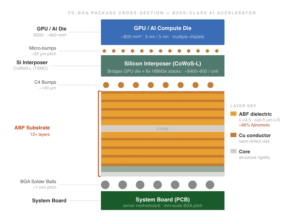
- Role & Function: Flip-Chip Ball Grid Array (FC-BGA) substrates act as the high-density spatial transformer connecting micro-pitch AI GPUs and CPUs (30–150 µm) to system boards (0.5–1.0 mm).
- Core Technology: Built on BT resin or glass-epoxy cores using Ajinomoto Build-up Film (ABF) to enable the semi-additive process (SAP), forming circuit traces down to 8/8 µm line/space across 12–20+ layers.
- Primary Yield Bottleneck: Coefficient-of-thermal-expansion (CTE) mismatch between copper (≈17 ppm/°C), ABF, and core materials causes severe panel warpage during reflow, especially in package sizes approaching 100 mm × 100 mm.
- Next-Gen Substrate Solutions: Low-CTE cores, symmetrical stack-ups, and emerging glass-core substrates offer high stiffness and flatness, though through-glass-via (TGV) plating and micro-cracking risks delay mass production.
- Supply Chain Risks: Ajinomoto Fine-Techno holds over 90% market share in qualified ABF film, while Tier-1 substrate manufacturing remains geopolitically concentrated across Japan (Ibiden, Shinko), Taiwan (Unimicron, Nan Ya), Korea (SEMCO), and Europe (AT&S).
FC-BGA substrates form the dense organic interconnect layer that connects fine-pitch server and AI chips to system boards. They use a rigid core made of Copper Clad Laminate (CCL)—a composite material constructed from bismaleimide-triazine (BT) resin or epoxy reinforced with woven glass fabric (known as prepreg)—with several build-up layers of Ajinomoto Build-up Film (ABF) laminated on top. ABF is an epoxy dielectric film that enables the semi-additive process (SAP) /Ajinomoto/. Fabricators laminate ABF, drill microvias (usually 30–50 µm) with lasers, desmear the surface, apply electroless copper, and electroplate the lines. This creates copper traces as fine as 8/8 µm line/space. Layer counts reach 12 to 20+ layers for high-I/O server GPUs and CPUs. The process requires high-purity copper deposition to create void-free vias and strong adhesion. It also requires precise layer alignment (±5 µm) across large panels. ABF’s surface chemistry supports this fine patterning where standard glass-reinforced prepreg fails. Ajinomoto holds a near-monopoly (roughly 90–98%) on qualified ABF film, making it a critical upstream material.
Warpage from coefficient-of-thermal-expansion (CTE) mismatch between copper (≈17 ppm/°C), ABF, and the core is the main cause of low yield /JLCPCB/. This problem worsens as substrate body sizes reach 100 mm × 100 mm or larger and layer counts increase for AI accelerators. Fine-line reliability, stacked-via integrity, and high-speed signal integrity create extra processing difficulties. Larger substrates increase alignment and plating uniformity challenges, so usable factory output often falls below installed capacity. New solutions include CTE-matched build-up films and cores, thicker low-CTE cores, symmetrical layer designs, and glass-core substrates /Yole/. Glass cores offer superior flatness and stiffness. However, glass introduces brittleness, through-glass-via (TGV) plating challenges, and handling risks that delay mass production.
High-Density FC-BGA Substrate & ABF Build-Up Process
Core Preparation & Drilling
Rigid BT / Glass-Epoxy SubstratePrepare a rigid copper-clad laminate core (BT resin or glass-epoxy) and drill mechanical through-holes for power and ground routing across large manufacturing panels (e.g., 515 mm × 610 mm).
ABF Lamination & Laser Via Drilling
Ajinomoto Build-Up Film LayeringLaminate layers of Ajinomoto Build-Up Film (ABF) dielectric onto the core and use UV or CO₂ lasers to drill tens of thousands of microvias (30–50 µm diameter).
Desmear & Electroless Copper Seed Layering
Chemical Surface PreparationChemically desmear laser-drilled microvia walls and deposit a thin electroless copper seed layer to provide electrical conductivity for electroplating.
Semi-Additive Process (SAP) Photolithography & Plating
Sub-10 µm Fine Circuit DefinitionApply photoresist, expose circuit patterns, and electroplate copper to define ultra-fine trace lines and spaces (down to 8/8 µm line/space) and fill microvias.
Multi-Layer Build-Up & Surface Finishing
12-to-20+ Layer Final AssemblyRepeat the ABF lamination, laser drilling, and SAP plating steps for up to 12–20+ layers, then apply solder mask, micro-bump pads, and surface finishes (ENEPIG/SOP).
AI and high-performance computing (HPC) servers drive most end-use demand. NVIDIA GPUs, AMD and Intel CPUs, custom ASICs/TPUs, and networking chips require large, high-layer FC-BGA substrates to handle high I/O density, power delivery, and thermal loads. Substrate surface area and layer counts for an advanced AI accelerator can be several times larger than those for a standard server CPU. This high demand extends supply tightness into 2027–2028 or beyond.
A small group of companies supplies the highest-end server and AI substrates: Ibiden and Shinko (Japan), Unimicron and Nan Ya PCB (Taiwan), Samsung Electro-Mechanics (Korea), and AT&S (Austria/Europe), with LG Innotek and others expanding capacity. Japan controls most ABF film production and premium manufacturing capability. Taiwan leads total production volume. This setup creates clear geopolitical concentration risks. Companies are building new facilities in Vietnam, Malaysia, Europe, and China. However, these new lines lag behind in qualifying the advanced high-layer, large-body substrates required for leading AI chips.
In practice, raw material bottlenecks hit substrate fabricators through sudden, broad-based cost surges across upstream Copper Clad Laminates (CCL) and prepreg. Because CCL cores rely on ultra-thin woven glass fabric as their primary structural backbone, any scarcity in electronic-grade glass yarn immediately constrains CCL production. Below is a real-world example of what the glass fabric bottleneck looks like: a price increase notice issued by Nan Ya Plastics Corporation (Electronic Materials Division) announcing a 20–25% price adjustment for CCL and prepreg due to severe glass fabric shortages /Jukanlosreve/:
Dear Valued Partner,
Thank you for your long-term partnership and continuous support.
Since the beginning of this year, the global electronic materials market has been facing unprecedented challenges. Currently, the overall market supply and demand have fallen into a severe imbalance, with the prices of core raw materials experiencing a broad-based and continuous surge. Among these materials, the shortage of glass fabric has become exceptionally severe, leading to a widening supply gap month by month and triggering an uncontrollable escalation in procurement costs. Faced with these unprecedented cost pressures and the highly volatile material market, we have exerted every effort to absorb these costs internally. However, the current production costs have far exceeded our capacity. To ensure a stable long-term supply and maintain the highest product quality, we have no alternative but to make the difficult decision to adjust our prices accordingly.
We sincerely apologize for any inconvenience this may cause and highly appreciate your understanding of this extreme market situation. We remain committed to closely monitoring supply chain dynamics and working together with you to navigate these challenging market conditions.
This 20–25% price adjustment on Copper Clad Laminates (CCL) and prepreg demonstrates how glass fabric supply gaps transmit directly into substrate core manufacturing, exacerbating cost pressures across the PCB and advanced packaging ecosystems and accelerating industry efforts toward alternative core materials like glass-core substrates.
Key Insights
What are the FC-BGA substrate volume and surface area requirements for next-generation AI accelerator architectures like NVIDIA’s Vera Rubin NVL72 or AMD Helios?
AI accelerator architectures like NVIDIA’s Vera Rubin NVL72—which integrates 72 dual-die Rubin GPUs and 36 Vera CPUs per rack—demand unprecedented FC-BGA substrate surface areas, typically exceeding 100 mm × 100 mm to 120 mm × 120 mm per GPU package with layer counts reaching 18 to 24+ layers. At an aggregate level, a single NVL72 rack consumes 4 to 6 times the total Ajinomoto Build-up Film (ABF) dielectric surface area of a legacy H100 or conventional server deployment. With initial shipment estimates reaching 5,000–7,000 Vera Rubin racks, global high-layer FC-BGA substrate consumption for frontier AI compute is projected to grow at a >25% CAGR, sustaining structural supply tightness across Tier-1 substrate suppliers through at least 2028.
What is the most critical process bottleneck in manufacturing advanced FC-BGA substrates for AI accelerators?
The single most critical process bottleneck is maintaining precise layer-to-layer alignment (±5 µm) and void-free microvia electroplating across large 515 mm × 610 mm manufacturing panels while managing thermo-mechanical warpage. Because expansion mismatches between copper traces (≈17 ppm/°C), ABF dielectric layers, and core resins induce non-planar twisting during 240–260°C reflow, large substrate bodies (>70 mm × 70 mm) suffer severe yield drops. Furthermore, drilling tens of thousands of microvias (30–50 µm) with CO₂ or UV lasers and desmearing residue across 16–20+ layer stack-ups require extremely narrow process windows, causing usable factory output to frequently fall 20–40% below installed physical capacity.
What are the unit economics, cyclicality, and margin defensibility of high-end FC-BGA substrates?
High-end FC-BGA substrates command premium gross margins (often 35–50% for leading-edge AI packages compared to 15–20% for standard PC packaging) due to extreme manufacturing barriers to entry and multi-year customer qualification cycles. Substrate fabricators protect against broader semiconductor market cyclicality by locking in multi-year Long-Term Supply Agreements (LTSAs) with major silicon vendors (such as NVIDIA, AMD, and Intel), frequently backed by customer capital expenditure co-investments or non-recurring engineering (NRE) prepayments to guarantee dedicated panel capacity. Margin defensibility remains high because of strict customer qualifications tied to specific ABF film formulations and high switching costs, allowing Tier-1 suppliers like Ibiden, Shinko, and Unimicron to retain pricing power even during PC or mobile market contractions.
What is Copper Clad Laminate (CCL), and how does an upstream glass fabric shortage trigger a 20–25% price increase across FC-BGA substrate core materials?
Copper Clad Laminate (CCL) is the foundational structural core of PCBs and FC-BGA substrates, manufactured by impregnating woven glass fabric with epoxy or bismaleimide-triazine (BT) resin (forming prepreg) and sandwiching it between thin copper foils under heat and pressure. Because electronic-grade woven glass fabric provides the essential mechanical reinforcement and dimensional stability for CCL cores, severe glass fabric supply deficits directly cap CCL and prepreg manufacturing volumes. When upstream glass yarn availability tightens, raw material suppliers face immediate cost escalation that propagates downstream—resulting in broad-based price adjustments of +20–25% for CCL and prepreg that inflate baseline package core manufacturing costs for substrate fabricators.