300mm Silicon Wafers: The Precision Foundation Powering AI Chip Production
- David Rogers
- AI Buildout Supply Chain
- 2026-07-08
NEED TO KNOW
- Substrate Foundation of AI: Every advanced AI GPU, TPU, and HBM stack is fabricated on a 300mm single-crystal silicon wafer pulled via the Czochralski (CZ) process from 9N–12N polysilicon.
- Japan Controls >50% Market Share: Shin-Etsu and SUMCO control ~50–54% of global 300mm wafer output, while the top five global suppliers command ~85% of market volume.
- 450mm Pivot Deprioritized: Equipment redesign costs led the semiconductor industry to abandon 450mm transitions, focusing instead on 300mm speed, hot-zone automation, and nanometer flatness.
- High Kerf Loss & Reclaim: Slicing boules into 300mm wafers incurs ~40% kerf loss, driving investment in diamond-wire technology and wafer reclaim processes.
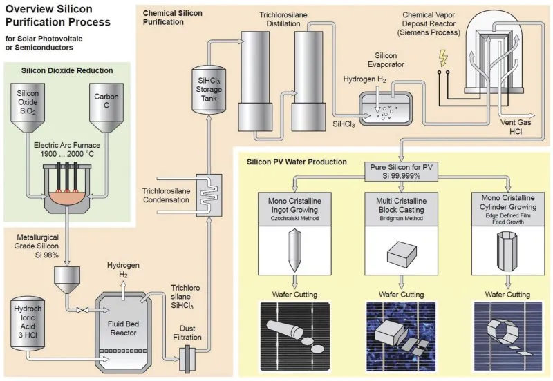
Every advanced AI processor and memory chip starts as a 300mm silicon wafer. A wafer is an atomically smooth, single-crystal silicon disk /NIST/. Producers refine quartz sand into ultra-pure polysilicon feedstock /Wacker/. Workers melt this polysilicon at 1,414 °C and pull a seed crystal to grow a heavy silicon ingot. Technicians slice the ingot into thin disks and polish them to sub-nanometer smoothness. This structural perfection determines manufacturing yields for sub-3nm microchips.
300mm Silicon Wafer Manufacturing Process
Chemical Polysilicon Refining
Siemens ProcessConvert raw quartz sand into 99.9999999% pure electronic-grade polysilicon gas and rods.
Czochralski Ingot Growth
Silicon Crystal PullingMelt polysilicon at 1,414 °C inside high-purity quartz crucibles and pull a large single-crystal ingot.
Diamond-Wire Slicing
Wafer FormattingCrop and slice the heavy silicon ingot with high-speed diamond wire to form thin 300mm silicon disks.
Chemical-Mechanical Polishing
Surface Flatness FinishingLap, etch, and polish raw silicon disks until the surface is atomically flat for sub-3nm AI chip fabrication.
The core challenges are technical and economic. Controlling oxygen incorporation from the crucible, dopant uniformity across 300mm diameters, and grown-in defects (COPs, slip) becomes exponentially harder at leading-edge nodes /SSRN/. Slicing still incurs ~40% kerf loss /Zelatec/; while diamond-wire technology and reclaim/recycling pilots recover material for solar or lower-grade use, closed-loop semiconductor-grade recovery remains limited and costly. Energy intensity of CZ growth and the multi-billion-dollar capex for new capacity add pressure. The industry has largely deprioritized 450 mm wafers /SemiWiki/ due to equipment scale-up costs, instead squeezing more value from 300mm through faster pull rates, better hot-zone design, automation, and ultra-flat specifications tailored for EUV and chiplet architectures.
Demand is tightly coupled to the AI buildout. 300mm wafers already represented over 64% of global silicon wafer area shipments (which reached ~12,266 MSI in 2024 and rebounded ~5–6% in 2025). AI accelerators, HPC logic, HBM, and advanced packaging are the primary drivers, with foundries and memory makers expanding capacity aggressively. Analysts project 5–7% CAGR for the silicon wafer market through the early 2030s as data-center and edge-AI silicon demand compounds /Fortune Business Insights/.
Supply is highly concentrated. Japan’s Shin-Etsu and SUMCO together supply roughly 50–54% of global 300mm wafers /Brookings/; the top five producers (adding GlobalWafers of Taiwan, Siltronic of Germany, and SK Siltron of Korea) control ~82–85%. Raw quartz is plentiful worldwide, but the know-how and capital for large-diameter, low-defect crystal growth create real bottlenecks. Wafer reclaim and kerf recycling provide marginal relief but do not meaningfully displace primary production. Geopolitical concentration risks are material: East Asia dominates both production and consumption (especially Taiwan’s advanced fabs), while China leads overall polysilicon capacity (mostly solar-grade) and is expanding domestic wafers under state support. Allied export controls on equipment and CHIPS Act-driven U.S. investments /Reuters/ are actively reshaping the map toward greater resilience.
For the AI industrial buildout, 300mm silicon wafers are foundational infrastructure. Without reliable volumes of these ultra-precise substrates, the GPUs and custom ASICs powering the next wave of intelligence cannot scale. Ongoing Japanese technology leadership, selective reshoring, process innovation to cut waste and cost, and diversified capacity will determine whether the physical layer keeps pace with AI’s software-defined ambitions.
Key Insights
How are 300mm silicon wafers manufactured for advanced AI chips?
Production begins by melting hyperpure electronic-grade polysilicon in a quartz crucible at 1,414 °C and using the Czochralski process to pull a single-crystal silicon ingot. This ingot is cropped, sliced using diamond-wire technology, lapped, and chemically-mechanically polished to achieve the nanometer flatness and parts-per-billion purity required for advanced node fabrication.
Why did the semiconductor industry deprioritize the shift to 450mm wafers?
The transition to 450mm wafers was deprioritized due to the massive capital expenditure required to redesign fabrication equipment and the high technical challenges of maintaining thickness uniformity across larger crystal diameters. Instead, manufacturers optimize 300mm wafer output using faster pull rates, improved crucible hot-zone designs, and automation.
Which companies dominate the global supply of 300mm silicon wafers?
Japanese specialists Shin-Etsu and SUMCO control 50% to 54% of the global 300mm silicon wafer market, while the top five global producers control up to 85% of total supply. This high concentration of processing expertise in East Asia represents a critical supply risk for global semiconductor foundries fabricating AI accelerators.
Are supply constraints emerging for 300mm (12-inch) silicon wafers?
Yes. In August 2026, Taiwan's GlobalWafers formally acknowledged supply constraints in 12-inch (300mm) silicon wafers as production lines reached maximum utilization across 300mm, 200mm, and 150mm lines. Tightening supply is driven by surging demand for AI chips, high-bandwidth memory (HBM), silicon photonics, and advanced packaging, prompting customers to secure long-term agreements (LTAs) spanning up to 5–10 years and driving up spot market prices.