HBM Stacking & Packaging Explained: Architecture, Yields, & Market Outlook
- David Rogers
- AI Buildout Supply Chain
- 2026-08-11
NEED TO KNOW
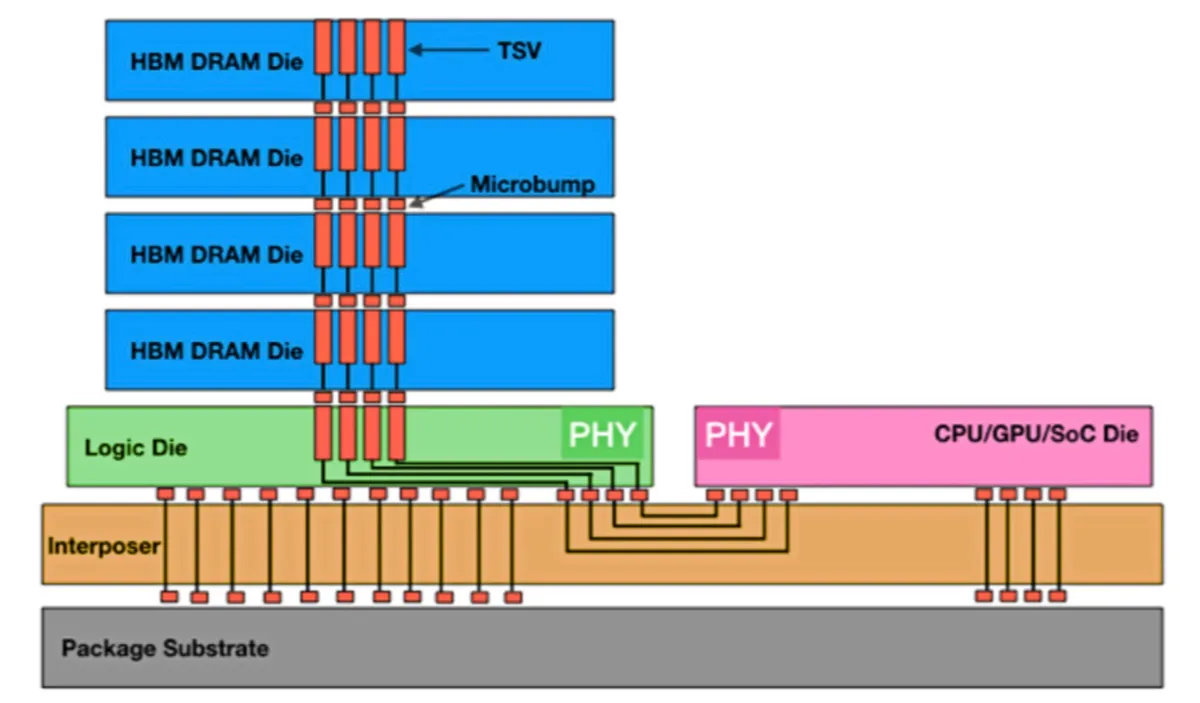
- Vertical Architecture & Standard Specifications: High-Bandwidth Memory (HBM) uses 3D-stacked thinned DRAM dies (~20–50µm) linked via Through-Silicon Vias (TSVs) and microbumps over a logic base die, connecting to accelerators through 2.5D interposers like TSMC CoWoS.
- JEDEC Relaxation for HBM4: JEDEC expanded the package height specification from 720 µm to 775 µm for HBM4, enabling 12-Hi and 16-Hi stacks without immediately requiring Cu-Cu hybrid bonding.
- Vendor-Specific Bonding Methodologies: Packaging strategies diverge across the core oligopoly—SK Hynix utilizes Mass Reflow Molded Underfill (MR-MUF), while Samsung and Micron rely on Thermocompression Bonding with Non-Conductive Film (TCB-NCF).
- Deferred Adoption of Hybrid Bonding: Direct copper-to-copper hybrid bonding offers lower heights and higher thermal conductivity, but high costs, sub-nanometer surface roughness requirements, and complex Known Good Die (KGD) testing have pushed its mainstream adoption past initial HBM4 to future nodes.
- Compound Manufacturing Challenges: Stack yields follow multiplicative loss dynamics across successive bonding steps, where ultra-thin dies escalate mechanical warpage and microbump pitches scaling below 10–20 µm increase power integrity and bridging risks.
- DRAM Capacity Displacement: HBM dies consume 2.5× to 3× the wafer area of standard DDR5 dies due to TSV keep-out zones and base logic integration, causing HBM production allocations to crowd out conventional DRAM supply.
- Geopolitical Supply Chain Vulnerabilities: Front-end HBM wafer fabrication remains heavily concentrated in South Korea (SK Hynix and Samsung), while back-end 2.5D packaging is anchored in Taiwan (TSMC), creating critical geographic bottlenecks for global AI hardware rollouts.
High-bandwidth memory (HBM) stacking is the vertical assembly of multiple thinned DRAM dies /Lam Research/. Through-silicon vias (TSVs) and microbumps (or emerging hybrid bonds) connect these dies electrically. The stack sits on a logic base die and connects to AI accelerators through silicon interposers such as TSMC’s CoWoS. TSVs formed by a via-middle process provide dense power and signal paths for the wide interface (1,024-bit scaling to 2,048-bit). However, bonding methods differ by vendor: SK Hynix uses mass-reflow molded underfill (MR-MUF) for productivity and heat control /SK/; Samsung and Micron use thermocompression bonding with non-conductive film (TCB-NCF). Overall, HBM represents a large share of total GPU build costs.

Key technical challenges center on compound yield loss, thermo-mechanical stress, and heat removal. Total stack yield drops as each bonding step adds defect risks /Semiconductor Engineering/. Hybrid copper-to-copper bonding provides shorter interconnects, lower stack height, better thermal conduction, and higher density. However, manufacturers postponed hybrid bonding past initial HBM4 due to strict surface roughness limits, particle controls, tight thermal budgets, difficult testing of known-good dies, and high costs /Semiconductor Engineering/. Engineers are studying alternative choices like side-stacking and direct 3D logic-memory integration /IEEE/. Commercial high-volume production still depends on improving TSV and microbump processes and expanding specialized tools.
| Generation | Data Rate (Gb/s) | Interface Width (b) | Bandwidth per Device (GB/s) | Stack Height | Max. DRAM Capacity (Gb) | Max. Device Capacity (GB) |
|---|---|---|---|---|---|---|
| HBM | 1.0 | 1024 | 128 | 8 | 16 | 16 |
| HBM2 | 2.0 | 1024 | 256 | 8 | 16 | 16 |
| HBM2E | 3.6 | 1024 | 461 | 12 | 24 | 36 |
| HBM3 | 6.4 | 1024 | 819 | 16 | 32 | 64 |
| HBM3E | 9.6 | 1024 | 1229 | 16 | 32 | 64 |
| HBM4 | 8.0 | 2048 | 2048 | 16 | 32 | 64 |
| HBM4E | 16.0 | 2048 | 4096 | 16 | 32 | 64 |
Source /Rambus/
End-use demand comes mostly from AI accelerators (NVIDIA platforms like Blackwell and Vera Rubin, AMD Instinct, Google TPUs, and custom ASICs) and high-performance computing. Bandwidth and capacity per stack continue to increase (multi-TB/s and tens to hundreds of GB), as AI data centers require more memory per system /EI/. Industry analysts project strong HBM market growth through 2026–2027 /IDC/. Multi-year contracts fully reserve production capacity, so customers often receive less volume than requested. HBM production also reduces standard DRAM supply because manufacturers shift silicon wafers to HBM.
Three suppliers control HBM production: SK Hynix, Samsung, and Micron /Counterpoint Research/. Factories cannot add significant new wafer capacity until late 2027–2028 despite large investments in South Korea. TSV processing tools remain a major bottleneck when converting standard DRAM lines /Mordor Intelligence/.
Geopolitical risks are high: South Korea produces most HBM wafers, Taiwan dominates advanced packaging (where TSMC CoWoS capacity limits final assembly) /EI/, and the United States has no local HBM wafer fabrication. Chip designers (especially NVIDIA) and the broader AI market depend on an East Asian supply chain vulnerable to regional conflicts, power disruptions, and specialized material shortages (such as underfill resins) /MK/. Supplier expansion plans reduce some risk, but dependency on South Korean memory and Taiwanese packaging will continue for years.
Key Insights
What are the HBM volume and capacity requirements in next-generation AI accelerator architectures like NVIDIA Vera Rubin NVL72 and AMD Helios?
In next-generation rack-scale AI architectures, HBM volume density scales dramatically to support massive frontier model parameters and long-context windows. NVIDIA’s Vera Rubin NVL72 platform incorporates 288 GB of HBM4 per Rubin GPU (20.7 TB of total HBM4 per 72-GPU rack), driving memory to account for over 60% of the Superchip’s Bill of Materials (BOM) cost. Similarly, the AMD Helios rack-scale architecture integrates 72 Instinct GPUs carrying up to 432 GB of HBM4 per GPU for a total of 31 TB of HBM4 capacity per rack. Across both ecosystems, HBM memory intensity expands at more than 2× per hardware generation, requiring the silicon equivalent of thousands of smartphones per enterprise AI cabinet.
What is the most critical process technology bottleneck in high-volume HBM manufacturing and advanced packaging?
The most severe process bottleneck in HBM scaling resides in high-aspect-ratio Through-Silicon Via (TSV) etch/fill tooling alongside sub-micron 2.5D/3D assembly precision. Etching millions of defect-free TSVs through thinned (~20–50µm) DRAM silicon requires specialized deep reactive-ion etching (DRIE) and dual-sided chemical-mechanical planarization (CMP) equipment that cannot be quickly retrofitted onto standard commodity DRAM lines. Furthermore, as microbump pitches scale toward 10–20µm and stack counts reach 12-Hi to 16-Hi under JEDEC height constraints (775µm for HBM4), thermal compression bonding with non-conductive film (TCB-NCF) and mass-reflow molded underfill (MR-MUF) face multiplicative yield degradation driven by die warpage compounding and particle contamination.
How do long-term supply agreements and structural capital intensity impact HBM unit economics and margin defensibility?
Unlike commodity DRAM, which suffers from severe spot-market cyclicality, HBM unit economics operate under custom multi-year take-or-pay long-term supply agreements (LTSAs) that fully allocate supplier manufacturing capacity up to two years in advance. Because HBM dies require 2.5x to 3x the silicon wafer area of standard DDR5 dies—due to TSV keep-out zones, complex logic base dies, and lower compound stack yields—producers command structural gross margin premiums often exceeding 50% to 60%. These gross margins are defended by steep technological barriers, proprietary thermal underfill intellectual property (such as SK Hynix’s MR-MUF), and high capital expenditure requirements for specialized 3D wafer-level packaging, insulating primary suppliers from traditional memory down-cycles.
How do evolving long-term supply agreement (LTSA) structures alter HBM market dynamics across full macro demand cycles?
While historical DRAM cycles suffered from extreme spot-market volatility and supply-demand mismatches, HBM's shift toward multi-year, non-cancellable LTSAs with advance customer prepayments fundamentally restructures memory market dynamics. By requiring hyperscalers and chip designers to lock in multi-billion-dollar capacity allocations up to two years ahead, memory suppliers shift volume risk upstream, securing the capital expenditure visibility required for dedicated 3D wafer-level packaging fabs. However, if AI infrastructure spending experiences a macro "digestion phase," rigid take-or-pay commitments could force hyperscalers to absorb underutilized inventory or attempt pricing renegotiations, while memory makers maintain margin protection through fixed-volume commitments. Over a full demand cycle, these structural contracts flatten traditional short-term memory boom-and-bust price swings, replacing them with longer-horizon structural capacity allocation shifts between enterprise HBM and consumer DRAM.
How are record AI profits impacting labor relations, profit-sharing disputes, and operational strike risks at leading memory producers like SK Hynix and Samsung?
The unprecedented profit surge driven by HBM demand has transformed labor-management dynamics at top memory makers, shifting worker compensation demands from traditional wage hikes to mandatory, uncapped operating profit-sharing pools. At SK Hynix and Samsung Electronics, unions successfully negotiated or demanded agreements locking in 10% to 10.5% of semiconductor operating profits for employee performance bonuses. However, as projected earnings reached record highs, management efforts to cap cash outflows—such as proposing partial stock-based bonus payouts—triggered fierce union backlash, organizing drives for unified labor unions, and threatened strikes across critical fab networks. These labor disputes highlight a structural cost overhang in the HBM supply chain, where talent retention and profit-sharing friction directly impact fab operational continuity and capacity expansion timelines during peak AI demand cycles.