Understanding Semiconductor Etch Machinery: Dry vs. Wet Processes in Advanced Chipmaking
- David Rogers
- AI Buildout Supply Chain
- 2026-07-24
NEED TO KNOW
- Atomic-Scale Anisotropy vs. Isotropy: Dry plasma etch uses energetic ions for directional vertical carving; wet chemical etch uses liquid baths for high-selectivity isotropic stripping.
- 3D NAND High-Aspect-Ratio Challenge: Etching 60:1+ channel holes in 3D NAND and 2nm GAA nanosheets requires cryogenic plasma etch tools and Atomic Layer Etching (ALE).
- Fab Capex Intensity: Etch machinery represents over 20% of total wafer fab equipment (WFE) spend, driven by Lam Research, Applied Materials, TEL, and AMAT.
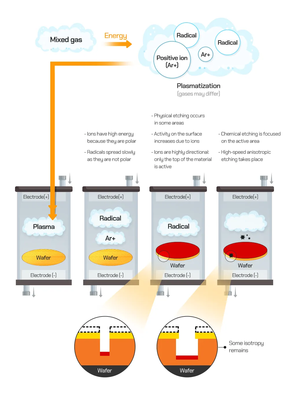
Semiconductor etching machines carve microscopic patterns into silicon wafers to build AI microchips /sk hynix/. Foundries use two main etching methods: dry plasma etching and wet chemical etching. Dry plasma etching uses energized gas ions to cut straight vertical channels into silicon. Wet chemical etching uses liquid acid solutions to strip away unneeded chemical layers evenly.
Plasma etch, dominated by reactive ion etching and inductively coupled plasma systems, acts as the industry’s precision laser. By energizing gases into a plasma state, these tools blast ionized particles straight down into a wafer to achieve strict vertical, directional cuts. This capability is non-negotiable for the towering vertical architecture of modern chips, such as 3D NAND memory cells with depth-to-width ratios that exceed one hundred to one /Phys/, or the delicate vertical channels of Gate-All-Around nanosheets.
Selective wet chemical etching functions as a chemical process. Liquids, such as hydrofluoric acid for silicon dioxide or phosphoric acid for silicon nitride, react with unmasked material to remove it. Wet etching operates isotropically, dissolving material equally in all directions. Fabs use wet etching to clear large areas, strip entire films, or clean wafers between process steps. However, as feature sizes shrink below 10 nanometers, liquid surface tension can collapse tiny structures, making wet etching unsuitable for fine vertical patterns /ResearchGate/.
Semiconductor Plasma & Chemical Etching Process
Chamber Gas Ionization
RF Plasma IgnitionPump reactive etching gases into a vacuum chamber and apply radio-frequency power to generate plasma.
Anisotropic Plasma Etching
Vertical Trench CarvingAccelerate energetic plasma ions vertically down into the wafer to carve high-aspect-ratio holes and trenches.
Selective Wet Chemical Stripping
Isotropic Layer RemovalImmerse wafers in liquid acid baths to dissolve unneeded sacrificial oxide layers without damaging silicon.
Atomic Layer Etch & Rinse
Sub-Nanometer PrecisionRemove material one atomic layer at a time, followed by a clean deionized water rinse and dry cycle.
Yet, pushing chip design to two nanometers and beyond creates severe physical bottlenecks. As aspect ratios exceed 60:1 in 3D NAND memory and GAA nanosheets, ions struggle to reach the bottom of deep features without distorting sidewalls /Lam Research/. Aspect-ratio-dependent etching causes deeper holes to etch more slowly than shallow ones. Meanwhile, liquid surface tension in wet etching causes delicate nanostructures to bend and stick together. To overcome these limits, chipmakers are adopting cryogenic plasma etching, which cools wafers to sub-zero temperatures to protect sidewalls, alongside atomic layer etching (ALE) for removal of single atomic layers.
This technological revolution is fueling massive financial growth, driven by the explosive demand for advanced artificial intelligence hardware, high-bandwidth memory (HBM), and ultra-dense storage chips. The semiconductor etch equipment market, valued at ~$25 billion in 2025 is projected to expand to ~$40 billion by 2031 /Mordor Intelligence/. Momentum stems from the sharp rise in etch steps needed for sub-3 nm logic, the transition to gate-all-around transistors, the vertical scaling of 300-plus-layer NAND, and high-bandwidth memory stacks that demand through-silicon vias /EI/ with aspect ratios above 100:1. Memory applications already accounted for nearly 40% of 2025 revenue, while advanced packaging and HBM are expected to grow even faster, underscoring etch’s critical role in enabling denser, higher-performance AI silicon.
Despite this economic momentum, the industry sits on fragile geopolitical ground. Tool manufacturing is dominated by a tight oligopoly led by Lam Research, Tokyo Electron, and Applied Materials, alongside specialized players like SCREEN, Hitachi High-Tech, and Chinese manufacturers like AMEC (Advanced Micro-Fabrication Equipment) and NAURA. As Western export restrictions tighten /CNBC/, domestic Chinese suppliers are rapidly establishing competitive alternatives. AMEC founder Gerald Yin Zhiyao noted that the company’s plasma-etching technology has reached industry-standard status across 65nm down to advanced 5nm and 3nm nodes, with tools adopted by global foundries including TSMC, while domestic champion SMIC has deployed over 800 AMEC etching machines in its fabs /SCMP/. On the chemical side, the raw material supply chain remains heavily reliant on fluorspar /EI/, the key feedstock for hydrofluoric acid used in both wet and dry processes, over sixty percent of which is mined in China. Because extreme chip purity requirements make gas recycling economically difficult, the global buildout of next-generation AI hardware remains deeply vulnerable to both high-tech equipment controls and raw material trade friction.
Key Insights
How many dry etch tools are deployed in leading-edge foundries like TSMC N2 or Intel 14A?
The transition to gate-all-around (GAA) nanosheets and backside power delivery at advanced sub-2nm nodes like TSMC N2 and Intel 14A increases etch process intensity by over 20%, requiring high-volume gigafabs to deploy hundreds of specialized dry etch chambers per 100,000 wafer-starts-per-month (WSPM) capacity. Major vendors like Lam Research maintain a global active installed base exceeding 90,000 chambers across logic, foundry, and memory fabs, with leading-edge nodes driving accelerated tool upgrades and new system installations to handle complex multi-patterning and atomic-layer etching workloads.
What is the most critical process bottleneck in modern semiconductor etch technology?
The defining process bottleneck in advanced etch technology is high-aspect-ratio (HAR) etching, where tools must carve deep vertical features exceeding 50:1 to 100:1 aspect ratios for 3D NAND memory holes and GAA channel releases without causing profile defects like bowing, necking, or twisting. Aspect-ratio-dependent etching (ARDE) restricts reactant gas delivery and byproduct removal at extreme depths, slowing material removal rates and degrading yield, which makes atomic layer etching (ALE) precision and pulsed RF energy control the ultimate limiting factors for sub-2nm chip manufacturing.
What are the unit economics, cyclicality, and margin defensibility of etch equipment manufacturers?
Etch machinery manufacturers operate with strong pricing power and high gross margins (~50%), defended by immense research and development barriers to entry and intimate co-development relationships with leading chipmakers. While tool shipment volumes remain tied to semiconductor capital expenditure cycles, suppliers mitigate cyclicality through long-term service agreements and high-margin recurring revenue from spare parts, software optimization, and chamber refurbishments—an installed-base support business that accounts for over a third of total revenue and provides resilient cash flow throughout industry downturns.