Why TSMC’s CoWoS and SoIC Advanced Packaging Bottleneck Global AI Accelerator Output
- David Rogers
- AI Buildout Supply Chain
- 2026-08-10
NEED TO KNOW
- The Primary AI Bottleneck: Wafer-level 2.5D and 3D advanced packaging—specifically TSMC’s CoWoS (Chip-on-Wafer-on-Substrate) and SoIC (System on Integrated Chips)—is the leading physical constraint on AI GPU and accelerator production.
- CoWoS vs. SoIC Mechanics: CoWoS uses micro-bump flip-chip bonding on a silicon interposer with deep reactive ion etched (DRIE) through-silicon vias (TSVs). SoIC uses true 3D hybrid direct copper-to-copper and dielectric bonding at sub-micron pitches, requiring ISO Class 1–2 cleanroom environments and sub-100nm overlay precision.
- Engineering & Yield Challenges: Key scaling obstacles include low silicon wafer material utilization (<70%), high interposer costs, thermal warpage on 120 mm × 120 mm packages due to silicon/organic CTE mismatch, and high particle sensitivity during hybrid bonding.
- Demand vs. Supply Capacity: Global CoWoS demand is projected to double from 1.3–1.4 million wafers in 2026 to 2.5–2.7 million in 2027. Even with TSMC reaching 120,000–140,000 monthly wafers by late 2026 and OSATs adding 50,000–60,000, supply will face a 10–20% shortfall.
- Emerging Alternatives & Geopolitics: Panel-level packaging (CoPoS) and glass substrates aim to reduce costs and warpage, but tool precision lags wafer-level readiness. With TSMC controlling ~95% of leading-edge 2.5D capacity in Taiwan, global AI hardware remains tied to acute geographic concentration risks through at least 2028–2029.
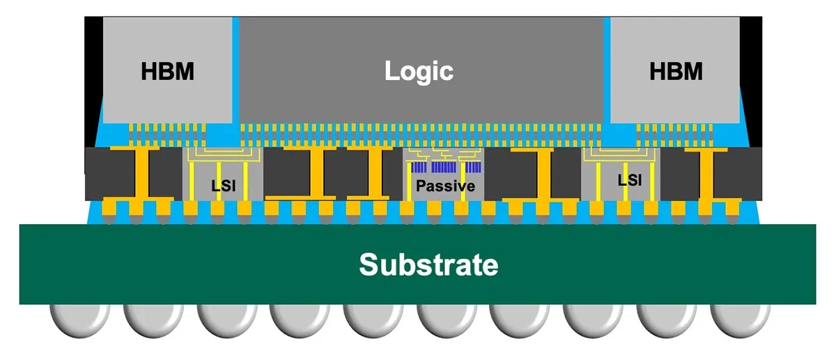
Wafer-level packaging through TSMC’s CoWoS (Chip-on-Wafer-on-Substrate) and SoIC (System on Integrated Chips) is now the main supply bottleneck for AI accelerator production. CoWoS builds a silicon interposer on a 300mm wafer using processes similar to front-end chip making. Deep reactive ion etching creates high-aspect-ratio through-silicon vias (TSVs). Machines then deposit insulating and barrier layers, add copper fill, and build multi-layer redistribution layers (RDLs) to provide dense, low-latency connections between logic dies and HBM stacks. Known-good dies attach to the wafer with micro-bump flip-chip bonding (Chip-on-Wafer). Workers then thin and dice the assembly, and workers bond the interposer to an organic substrate (Wafer-on-Substrate). SoIC advances this design into true 3D by using hybrid bonding /IEEE/. Direct copper-to-copper and dielectric-to-dielectric bonds join at sub-micron pitches. This process requires extremely flat surfaces, clean environments with almost zero particle contamination (ISO Class 1–2 cleanrooms), and alignment accuracy under 100nm. These steps require cleanroom purity and yield control far beyond traditional packaging.
TSMC CoWoS Interposer & Advanced Packaging Process
Wafer Size & Substrate Prep
CoWoS Interposer ProcessUses standard 300mm silicon wafers as the foundational interposer substrate.
Front-End Lithography & Deposition
CoWoS Interposer ProcessApplies photolithography, chemical vapor deposition (CVD), and copper plating to form high-density redistribution layers.
Through-Silicon Via (TSV) Etching
CoWoS Interposer ProcessEtches Through-Silicon Vias to route electrical signals vertically through the silicon interposer.
Backside Preparation & Thinning
CoWoS Interposer ProcessThins the silicon interposer wafer down to expose TSV contacts before bonding chips on top.
Chip Stacking & Micro-Bump Placement
Advanced Packaging StepsPlaces logic compute dies and High Bandwidth Memory (HBM) stacks onto the interposer using fine-pitch micro-bumps.
Substrate Mount & Integration
Advanced Packaging StepsAttaches the completed interposer assembly (Chip-on-Wafer) to a larger organic package substrate.
Protective Underfill Injection
Advanced Packaging StepsInjects protective polymer material underneath the mounted dies for mechanical strength and structural integrity.
Key technical challenges center on yield, cost, and scale. Silicon interposers are expensive, often costing more than half the total package. Reticle size limits interposer area, and circular-wafer edges waste material, keeping material utilization below 70% for large AI dies. Differences in the coefficient of thermal expansion between silicon and organic substrates cause thermal stress and warpage at package sizes near 120mm by 120mm. Hybrid bonding for SoIC is sensitive to particles and voids, which limited early yields until process improvements raised yields into the high 80–90% range on test vehicles. Emerging solutions include panel-level packaging (CoPoS) on larger rectangular substrates for better area efficiency, glass substrates to reduce warpage, active local silicon interconnect bridges, and more outsourcing of the CoW step. However, panel tools currently lack wafer-level precision, and high-volume production remains years away.
| Feature | CoWoS-S | CoWoS-R | CoWoS-L |
|---|---|---|---|
| Interposer Base | Full Silicon | Polymer RDL | RDL + Silicon Bridges |
| Wiring Density | Ultra-Fine (Sub-micron) | Medium | Fine (At Bridges) |
| Relative Cost | High | Low | Medium-High |
| Max Package Size | Restrained by reticle | Very Large | Extremely Large (Modular) |
| Nvidia Deployment | H100, H200, B100 | None | Blackwell (B200/GB200) & Vera Rubin (2026/2027) |
| AMD Deployment | MI300 series | None | Instinct MI400 series |
| Broadcom Deployments | High-performance custom nodes | Standard/Cost-sensitive networking ASICs | Multi-chip high-bandwidth custom logic |
| Google TPUs | TPU v4, v5p | None | Trillium (TPU v6e) (Note: Certain next-gen TPUs are shifting toward Intel’s EMIB) |
| Hyperscaler Custom ASICs | Early gen chips (e.g., MSFT Maia 100) | Meta MTIA v1 (non-HBM edge) | Meta MTIA v3, AWS Trainium 2/Inferentia |
End-use demand comes almost entirely from AI and high-performance computing accelerators. Nvidia (Blackwell/Rubin and successors), AMD (MI300/MI400 series), Broadcom, Google TPUs, and hyperscaler custom ASICs consume most of the capacity. Nvidia alone has booked roughly 50–60% of TSMC’s 2026 CoWoS output at the end of 2025 /DigiTimes/. Global CoWoS demand will double from about 1.3–1.4 million wafers in 2026 to 2.5–2.7 million in 2027. This growth rate outpaces near-term supply growth and keeps the technology central to every major AI training and inference platform, supporting forecasts that the broader semiconductor market will surpass $1.5 trillion driven by AI demand /Reuters/.
TSMC’s monthly CoWoS capacity will reach 120,000–140,000 wafers by the end of 2026 (up from roughly 70,000 in 2025). OSAT partners (ASE/SPIL, Amkor) will add another 50,000–60,000 wafers, bringing industry totals near 200,000 wafers per month. This total still leaves a 10–20% supply shortfall /UDN/. To narrow this gap, TSMC is constructing additional advanced packaging facilities in Chiayi, Taiwan /Reuters/, with plans already extending into secondary expansion phases. Capacity expansion has delivered compound annual growth above 80% since 2022, but lead times remain long and new production lines require 12–18 months to qualify.
TSMC holds approximately 95% of leading-edge 2.5D CoWoS capacity, which makes it the main processor for interposers and hybrid-bonded stacks. OSATs such as ASE, Amkor, and SPIL handle increasing volumes of licensed CoW and WoS steps, while Intel (EMIB/Foveros) and Samsung offer alternatives at smaller scale. This high geographic concentration in Taiwan creates significant geopolitical risk. Any supply disruption would immediately reduce global AI hardware output. This risk prompts U.S. and allied efforts to build domestic packaging capacity, like TSMC Arizona, but these facilities will not relieve the bottleneck before 2028–2029.
Key Insights
What are the volume estimates for CoWoS/SoIC packaging in architectures like NVIDIA’s Vera Rubin NVL72 or AMD’s Helios?
NVIDIA’s Vera Rubin NVL72 (72 Rubin GPUs + 36 Vera CPUs) and AMD’s Helios (72 MI455X GPUs) each require large CoWoS-L interposers—typically 2-reticle compute dies plus 8–12 HBM4 stacks per GPU package—driving multi-hundred-thousand wafer annual demand; NVIDIA alone is projected to consume ~1.22 million CoWoS wafers in 2027 (roughly 45–60% of global capacity), while AMD’s larger 5.5×-reticle MI455X packages with SoIC hybrid bonding add further pressure, with total industry CoWoS demand expected to roughly double from ~1.4 million wafers in 2026 to ~2.7 million in 2027.
What is the most critical bottleneck process technology in wafer-level packaging for these AI accelerators?
The most critical bottleneck is the high-precision Chip-on-Wafer (CoW) attachment and silicon-interposer fabrication (including TSV formation, multi-layer RDL, and hybrid bonding for SoIC), which demands sub-100nm alignment, near-zero particle contamination, and warpage control on packages approaching or exceeding reticle limits; these steps remain capacity-constrained at TSMC even after aggressive expansion, with hybrid-bonding cleanliness and large-interposer yield still limiting throughput far more than front-end wafer starts.
What are the unit economics of CoWoS/SoIC packaging, including long-term supply agreements, cyclicality, and margin growth/defensibility?
CoWoS wafer ASPs approach ~$10,000 (comparable to 7nm logic wafers) and support gross margins well above TSMC’s corporate average, reinforced by multi-year prepayment commitments (especially from NVIDIA locking >50% of capacity through 2027) that provide exceptional visibility and reduce cyclicality; structural AI demand, near-monopoly process control, and rising packaging contribution (projected to exceed 10% of TSMC revenue) create strong margin expansion and defensibility, as alternatives such as panel-level CoPoS remain years from high-volume readiness.
What is the difference between CoWoS and CoPoS packaging?
CoWoS (Chip-on-Wafer-on-Substrate) is TSMC’s mature wafer-level 2.5D technology that builds high-density silicon interposers on standard 300mm circular wafers using front-end-like processes (TSVs, fine-pitch RDL), delivering superior interconnect density and yield for today’s largest AI packages but suffering from edge waste and size limits imposed by the round wafer and reticle field. CoPoS (Chip-on-Panel-on-Substrate) shifts to larger rectangular panels (e.g., ~310 × 310mm) for better area utilization, lower cost per unit area, and the ability to accommodate even bigger multi-die assemblies; however, panel-level tools currently lag wafer-level processes in lithography precision, alignment accuracy, and interconnect density, so CoPoS remains in pilot stage with meaningful high-volume production not expected until 2028–2029.