3nm and 2nm Foundry Nodes: EUV, GAA Transistors, and AI Silicon Trends
- David Rogers
- AI Buildout Supply Chain
- 2026-08-06
NEED TO KNOW
- Core Lithography & Substrate Infrastructure: Sub-3nm chip manufacturing relies on ASML extreme ultraviolet (EUV) lithography systems, EUV multi-patterning, ultra-pure 300mm silicon wafers with sub-angstrom surface roughness, and Class-1 cleanrooms.
- Transistor Architecture Divergence: TSMC used FinFET for its N3 node before adopting Gate-All-Around (GAA) nanosheets for N2, while Samsung introduced GAA at 3nm and Intel is deploying its GAA RibbonFET with PowerVia backside power at 18A.
- Backside Power Delivery Trade-offs: Backside Power Delivery Networks (BSPDN) free up frontside metal routing layers and reduce IR voltage drop, but they introduce complex wafer-thinning, lithographic overlay alignment, and thermal management challenges.
- High-NA EUV Economic Thresholds: High-NA EUV (0.55 NA) increases single-exposure resolution to ~8 nm, but tool costs exceeding $350 million led TSMC to defer broad adoption for early 2nm in favor of 0.33 NA multi-patterning, while Intel and Samsung integrate High-NA earlier.
- Capacity Constraints Driven by AI Demand: Unprecedented demand for AI accelerators and custom hyperscaler silicon from NVIDIA, AMD, Apple, Qualcomm, Broadcom, Google, AWS, and Microsoft has fully booked 3nm and 2nm foundry capacity through 2026 and beyond.
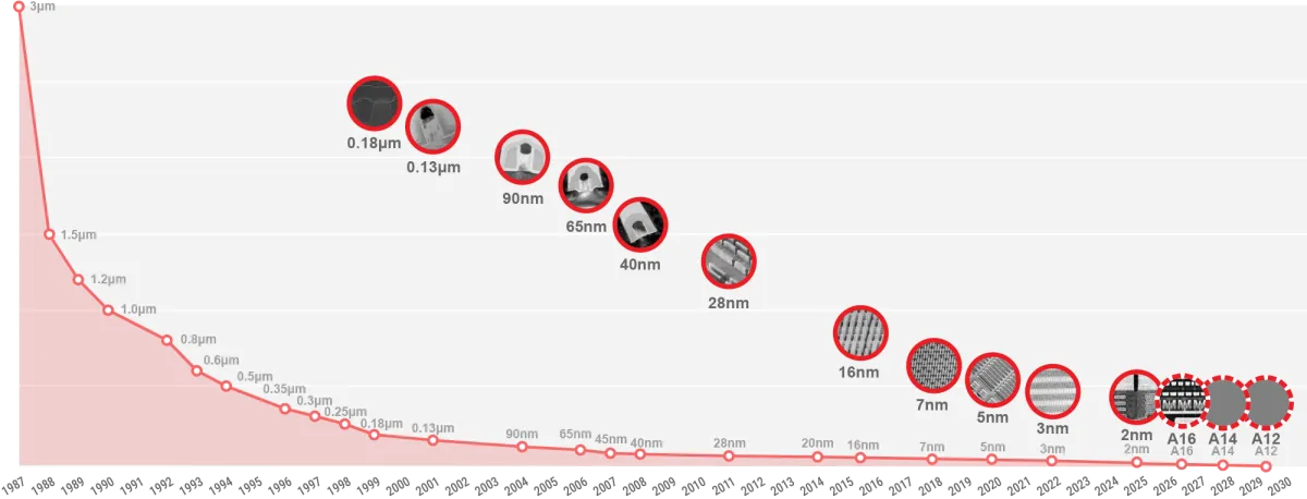
Leading-edge logic foundries at 3nm and 2nm form the front line of AI hardware development. These nodes require extreme ultraviolet (EUV) lithography—primarily from ASML tools—along with multi-patterning, ultra-pure 300mm silicon wafers (sub-angstrom surface roughness and near-zero defects from producers like Shin-Etsu and SUMCO), and class-1 cleanrooms. TSMC’s N3 remains a refined FinFET process that entered high-volume manufacturing earlier, while its N2 (volume production starting in late 2025) marks the company’s first Gate-All-Around (GAA) nanosheet transistors. Samsung introduced GAA earlier at 3nm, while Intel develops its own RibbonFET and PowerVia (backside power) variants. The purity and precision requirements are absolute: a single particle or alignment error can destroy yields on designs packing hundreds of millions of transistors per square millimeter.

The primary technical challenges are yield ramps, cost, and process complexity. Early N2 yields at TSMC are reported in the 65–80% range for logic test chips—a strong result for a first-generation GAA transition—yet still leave room for improvement as manufacturing scales up. Backside power delivery networks (BSPDN) free up frontside metal routing and reduce voltage drops, but they introduce wafer-thinning, via-alignment, and heat-dissipation issues that engineers must solve alongside the transistor stack /Applied Materials. High-NA EUV tools (0.55 NA) offer higher resolution and fewer multi-patterning steps for sub-2nm work, but each system costs hundreds of millions of dollars and increases per-wafer expense; TSMC has delayed wide adoption until later in the decade for economic reasons while Intel and Samsung move forward. Current industry efforts focus on higher throughput tools, advanced process control, and design-technology co-optimization (DTCO) to reduce cost, material waste, and cycle time.
The demand for these chips comes almost entirely from AI infrastructure investments. Companies like NVIDIA, AMD, Apple, Qualcomm, Broadcom, and hyperscalers building custom silicon (Google, Amazon, Microsoft) have reserved most 3nm and 2nm manufacturing capacity for AI accelerators, high-performance computing, and premium mobile processors. Advanced-node logic capacity is fully booked through 2026 and beyond; industry forecasts show this market segment growing at double-digit compound annual growth rates (CAGRs) as AI workloads transition to denser, more power-efficient transistors.

Installed manufacturing capacity remains constrained and concentrated. TSMC targets roughly 180,000 wafers per month of 3nm output by the end of 2026 and near 100,000 wafers per month of 2nm, with major customers booking both nodes completely. Samsung and Intel are expanding their operations, but they trail TSMC in total volume and yield maturity at these nodes. Japanese suppliers dominate raw silicon wafer production, but the main supply bottleneck remains the multi-billion-dollar EUV-equipped fabrication plants. Finally, advanced chip recycling and material recovery remain limited due to proprietary designs, complex 2.5D/3D packaging, and low overall scrap volumes at these leading nodes.
Key Insights
How do next-generation AI architectures like NVIDIA’s Vera Rubin NVL72 and AMD Helios impact 3nm/2nm wafer capacity and throughput utilization?
Next-generation rack-scale architectures such as NVIDIA’s Vera Rubin NVL72 (uniting 72 Rubin GPUs and 36 Vera CPUs) and AMD Helios (integrating 72 Instinct MI455X GPUs with EPYC "Venice" CPUs) require unprecedented volumes of leading-edge silicon per deployed system. Integrating hundreds of billions of logic transistors per rack alongside dense memory controllers drives 3nm and 2nm foundry throughput utilization to near 100% capacity across primary manufacturing lines. With TSMC targeting approximately 180,000 3nm wafers and 100,000 2nm wafers per month by late 2026, hyperscaler and enterprise demand for these multi-terabyte memory, high-density AI accelerators effectively locks up leading-edge wafer supply well into future production cycles.
What is the most critical bottleneck process technology in sub-3nm chip manufacturing?
The primary technical and economic bottleneck in sub-3nm manufacturing is high-cost, high-precision extreme ultraviolet (EUV) lithography—specifically managing overlay alignment, mask counts, and scanner availability. While High-NA EUV (0.55 NA) promises to reduce multi-patterning steps and improve sub-2nm feature resolution, individual tool costs approaching $400 million force foundries to extend standard 0.33 NA Low-NA EUV through complex multi-patterning steps to balance yield and capital expenditure. Combined with extreme physical integration constraints in Backside Power Delivery Networks (BSPDN)—such as carrier wafer bonding, sub-micron silicon substrate thinning, and thermo-mechanical stress—EUV lithography capacity and overlay precision remain the gating factor for scaling advanced logic throughput.
How do long-term supply agreements and cyclicality shape the unit economics and margin defensibility of sub-3nm logic components?
The unit economics of sub-3nm logic are defined by exceptionally high fixed capital expenditures, creating strong pricing power and gross margin defensibility (>50%–60%) for leading pure-play foundries and top-tier fabless designers. To derisk multi-billion-dollar fab expansions and insulate against broader semiconductor cyclicality, foundries secure long-term supply agreements (LTSAs) and non-refundable prepayments from major AI accelerator vendors. While initial per-wafer costs increase substantially at 3nm and 2nm due to complex yield learning curves and expensive EUV tooling, the extreme transistor density, performance-per-watt gains, and lock-in on custom AI silicon allow suppliers to pass higher wafer costs directly to hyperscalers, protecting operating margins across economic cycles.
How do advanced packaging techniques from TSMC, Intel, and Samsung address the bandwidth and interconnect bottlenecks in AI accelerator designs?
Advanced 2.5D and 3D packaging technologies are critical for bypassing physical reticle size limits and interconnect bottlenecks by integrating heterogeneous logic compute dies with High Bandwidth Memory (HBM) stacks in close physical proximity. TSMC leads the high-volume market with its CoWoS (Chip-on-Wafer-on-Substrate) interposer platform and 3D hybrid-bonded SoIC (System-on-Integrated-Chips). Intel competes via its localized silicon bridge architecture EMIB (Embedded Multi-die Interconnect Bridge) and 3D vertical stacking Foveros/Foveros Direct, offering alternative cost structures without requiring full-reticle silicon interposers. Samsung leverages its I-Cube (2.5D) interposer family and 3D SAINT (Samsung Advanced Interconnection Technology) platforms, positioning itself as a turnkey supplier combining in-house HBM manufacturing, wafer fabrication, and advanced packaging under one roof.