Indium Supply Chain Risks for AI Data Centers: InP Lasers & China’s Silicon Photonics Pivot
- David Rogers
- AI Buildout Supply Chain
- 2026-07-01
NEED TO KNOW
- Optical Interconnect Catalyst: Indium phosphide (InP) lasers and modulators power 800G and 1.6T transceivers, replacing copper as AI clusters exceed electrical reach and bandwidth limits.
- Extreme Substrate Oligopoly: Sumitomo Electric and AXT control ~80% of global InP substrate capacity, with 6-inch wafer prices surging 250% following Chinese export controls.
- Byproduct Mining Constraint: Primary indium is recovered only as a low-ppm byproduct of zinc refining, with China producing ~70% of world refined volume.
- Silicon Photonics & CPO Pivot: Hyperscalers and firms like Huawei are adopting Silicon Photonics (SiPh) and Co-Packaged Optics (CPO) with quantum dot lasers to minimize indium consumption per link.
Indium is emerging as a quiet but critical enabler of the AI buildout. While long used in indium tin oxide (ITO) transparent conductors for displays and touchscreens, its highest-stakes application today is in indium phosphide (InP) lasers, modulators, and photodetectors that drive high-speed optical interconnects in AI data centers. As copper hits physical limits on bandwidth, power, and reach, InP-based 800G and 1.6T transceivers (and future co-packaged optics) have become essential for moving massive data between GPUs and racks /Photonics Spectra/.
Primary indium is recovered almost exclusively as a byproduct of zinc refining from sphalerite ores (typically 1–100 ppm indium content). Zinc residues undergo concentration, then energy-intensive purification through vacuum distillation, electrolysis, and zone refining to reach the ultra-high purity (6N / 99.9999% or higher) required for InP crystal growth. High-purity indium is reacted with purified phosphorus to form polycrystalline material, which is then grown into single-crystal boules via Vertical Gradient Freeze (VGF), Vertical Bridgman, or Liquid-Encapsulated Czochralski (LEC) methods /10.15541/jim20220645/. These boules are sliced and polished into wafers (predominantly 6-inch today). The process is technically demanding due to phosphorus volatility, material brittleness, defect control, and low yields; scaling to larger wafers (toward 8-inch) is a key focus for cost reduction.
Global refinery production is heavily concentrated: China accounts for roughly 70% of world output (approximately 760 tonnes of capacity in recent data), with total world refinery production around 1,020 - 1,100 tonnes annually. The United States has no primary mine production and is 100% import-reliant for refined indium /USGS/. Major InP substrate producers form an oligopoly with Sumitomo Electric (Japan) and AXT (U.S., with significant China operations) controlling ~80% of global substrate capacity, and JX Advanced Metals adding another ~10%. Additionally, InP wafer consumers like Coherent and Lumentum are unlikely to switch suppliers easily, as qualifying a new source requires lengthy cycles of reliability testing, performance validation, and process integration that can take many months.
Thus, geopolitical risks have intensified. China’s 2025 export licensing and inspection requirements on indium and InP-related materials have caused sharp price spikes with 6-inch InP wafer prices rising 250% to around $5,000 and created delays for suppliers with China exposure, such as AXT /Reuters/. This comes as AI-driven demand surges: InP content per optical module nearly doubles when moving from 800G to 1.6T, and industry analyses project meaningful shortfalls in InP wafers and especially electro-absorption modulated laser (EML) lasers through 2027–2029 as hyperscalers standardize higher-speed optics /10.1088/1674-4926/25030015/.
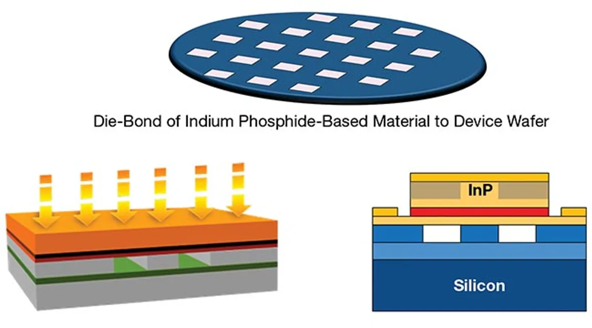
Chinese firms such as Huawei are actively mitigating Indium/InP constraints through alternative architectures centered on silicon photonics (SiPh) integration and co-packaged optics (CPO) that can be fabricated directly on silicon using high-volume CMOS processes. Huawei research focuses on low-voltage SiPh micro-ring modulators (>40 GHz bandwidth, ~1V drive) and Indium Arsenide/Gallium Arsenide quantum dot lasers (InAs/GaAs on Si) for on-chip or hybrid light sources, enabling dense, low-power optical I/O chiplets placed near AI ASICs to bypass conventional high-power serializer/deserializer (SerDes) copper traces power and material intensity. Commercial efforts, including InnoLight’s partnerships with Tower Semiconductor /Tower Semi/, deliver scalable SiPh-based 800G/1.6T transceivers and CPO solutions optimized for cost and volume. Domestically, InP substrate capacity is expanding rapidly (e.g., Yunnan Germanium targeting hundreds of thousands of wafers annually) alongside SiPh and thin-film lithium niobate (TFLN) modulator advances, creating a dual-track strategy that secures supply while reducing per-link Indium dependence and supporting sovereign, massive-scale AI cluster deployments.
Key Insights
What role does indium play in AI data center optical transceivers?
Indium is the primary element in indium phosphide (InP) lasers, modulators, and photodetectors that power high-speed 800G and 1.6T optical interconnects. As electrical copper connections face physical limitations at high bandwidths, InP-based transceivers are critical to enable low-power, high-speed data transmission between GPU clusters in AI networks.
What are the primary supply chain risks for indium and InP substrates?
China produces approximately 70% of the world's refined indium, and Chinese export controls implemented in 2025 have driven up 6-inch InP wafer prices by 250% to roughly $5,000. Furthermore, two companies, Sumitomo Electric and AXT, control about 80% of global InP substrate capacity, making it difficult for chipmakers to qualify alternative suppliers quickly.
How are technology companies mitigating indium supply risks in AI infrastructure?
Companies like Huawei are developing silicon photonics platforms and co-packaged optics (CPO) that integrate Indium Arsenide/Gallium Arsenide (InAs/GaAs) quantum dot lasers directly onto silicon handle wafers. By using standard CMOS fabrication processes, these designs minimize the amount of indium needed per optical link and bypass conventional high-power SerDes copper traces.