How Semiconductor Deposition (CVD, PVD, ALD) Builds AI Silicon
- David Rogers
- AI Buildout Supply Chain
- 2026-07-23
NEED TO KNOW
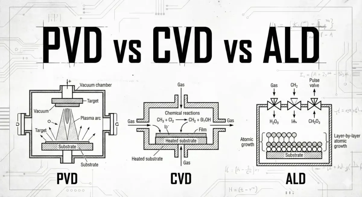
- The Big Three Deposition Techs: Chemical Vapor Deposition (CVD) provides high-throughput uniformity for oxides/nitrides (50–200 nm/min); Physical Vapor Deposition (PVD) sputters metal barriers (TiN, TaN) prioritizing purity; Atomic Layer Deposition (ALD) delivers sub-nanometer thickness control and >95% conformality in 100:1 aspect ratios.
- AI Architecture Drivers: Advanced chip designs like Gate-All-Around (GAA) logic add 15–20 deposition layers per wafer, alongside high-bandwidth memory (HBM) and backside power delivery needs.
- Market Projections: Driven by AI compute demand, the global thin-film deposition equipment market is expanding from ~$35B in 2025 toward $70–77B by the mid-2030s (7–8% CAGR), with ALD seeing the fastest growth rate (9–15% CAGR).
- Next-Gen Manufacturing: Emerging solutions like Area-Selective Deposition (ASD), spatial ALD, and direct-write Atomic Layer Additive Manufacturing (ALAM) aim to bypass lithography steps, eliminate edge-placement errors, and reduce chemical waste.
- Market Concentration: Strategic tooling is dominated by four global leaders: Applied Materials (>70% PVD market share), Lam Research (high-aspect-ratio memory tools), Tokyo Electron (PECVD/batch ALD), and ASM International (high-k metal gate ALD).
Thin-film deposition tools deposit microscopic material layers onto silicon wafers to build AI processors and 3D memory chips /Lam Research/. Chemical Vapor Deposition (CVD) uses chemical gases to deposit insulating and conducting films. Physical Vapor Deposition (PVD) sputters metal targets to create thin metal barriers and wiring seed layers. Atomic Layer Deposition (ALD) deposits material one atomic layer at a time, providing sub-nanometer thickness control inside deep 3D chip structures.
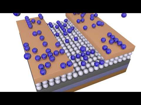
Atomic Layer Deposition (ALD) Monolayer Cycle
Precursor Gas Pulse
Surface ChemisorptionPulse organometallic chemical gas into a vacuum chamber until it forms a single layer of molecules on the wafer.
Inert Gas Purge
Excess Gas RemovalFlush the chamber with inert nitrogen gas to remove unreacted chemical gas molecules.
Co-Reactant Gas Pulse
Chemical Layer ReactionInject co-reactant gas into the chamber to react with the molecules and create an insulating or metallic film.
Secondary Purge & Cycle Repeat
Sub-Nanometer Layer GrowthFlush away chemical byproducts and repeat the process to build atomic-scale layers inside 3D memory and logic chips.
Throughput, conformality in extreme 3D geometries, and sustainability remain the core technical bottlenecks, possibly addressed by both evolutionary and direct-write advances /EETimes/. ALD’s precision comes at the cost of slow rates (0.5–2 nm/min), while high-aspect-ratio features demand uniform coverage without voids or plasma damage; thermal budgets are tightening as devices stack. Emerging solutions include spatial ALD and hybrid ALD/CVD for higher throughput, microwave-plasma ALD for dense, low-damage films, area-selective deposition that grows material only where needed /Applied Materials/, and direct-write techniques such as atomic layer additive manufacturing (ALAM) /RSC/. ALAM adapts ALD’s self-limiting chemistry to a scanning precursor nozzle that “prints” material in a 3D-printing mode, enabling maskless, atom-by-atom patterning with reduced precursor consumption and without relying on inhibitors or pre-patterned substrates including cutting lithography steps, waste, and edge-placement errors /Atlant 3D/. Green CVD initiatives further cut precursor use 20–60% and greenhouse gases such as NF₃ and N₂O by 25–67%, while precursor recovery and cylinder reuse trim costs.
AI compute demand is the dominant growth engine. Gate-all-around logic, high-bandwidth memory, and backside power delivery each multiply deposition steps as GAA alone can add 15–20 new layers per wafer, pushing the overall thin-film deposition equipment market from roughly $35 billion in 2025 toward $70–77 billion by the mid-2030s at 7–8% CAGR. Within this, CVD remains the largest-volume segment for high-throughput dielectrics, polysilicon, and fills /Grand View Research/, while ALD is the fastest-growing precision segment (roughly $5–8 billion and rising, with CAGRs of 9–15% in many forecasts) driven by the need for conformal high-k dielectrics, spacers, barriers, and liners in GAA, 3D NAND, and advanced interconnects /Mordor Intelligence/. Memory and advanced packaging for accelerators further amplify these needs, especially for molybdenum wordlines and low-k films.
Equipment capacity is highly concentrated among a handful of firms, creating both capability and geopolitical exposure. Applied Materials (U.S.) leads overall with dominant PVD share (>70% in key segments) /Applied/ and strong CVD/ALD platforms; Lam Research (U.S.) excels in high-aspect-ratio CVD and ALD for memory /Lam/; Tokyo Electron (Japan) holds key positions in PECVD and batch ALD /Tokyo Electron/; ASM International (Netherlands) is the specialty ALD leader for high-k metal gates /ASM/. Chinese suppliers such as NAURA and AMEC serve mature nodes but lag at leading-edge precision. Export controls already restrict advanced tools to China, while precursor qualification lock-in (6–12 months) and occasional supply disruptions underscore concentration risk. Recent European consolidation includes Jolt Capital’s €20M investment in Tempress (Netherlands), enabling its acquisition of SPT Microtechnologies USA to strengthen thermal CVD, LPCVD, and ALD furnace offerings for power, SiC, MEMS, and photonics segments /EIN/.
In short, deposition is the precision manufacturing process step that will determine how densely and efficiently AI silicon can be built. As logic architectures shrink to atomic scales and memory stacks reach hundreds of layers, the ability to control film growth at the sub-nanometer level dictates both chip performance and yield. Fabs that master these thin-film deposition techniques will directly shape the compute power, energy efficiency, and overall pace of the AI revolution.
Key Insights
What is the estimated tool volume and installed base for deposition equipment in advanced foundry nodes like TSMC N2 and Intel 18A?
In leading-edge foundry nodes like TSMC N2 (2nm) and Intel 18A (1.8nm), thin-film deposition equipment accounts for 20–25% of total wafer fab equipment (WFE) spend. A standard mega-fab module producing 50,000 wafer starts per month (WSPM) at these sub-2nm nodes requires an estimated installed base of 180 to 240 specialized deposition chambers spanning Chemical Vapor Deposition (CVD), Physical Vapor Deposition (PVD), and Atomic Layer Deposition (ALD). The introduction of Gate-All-Around (GAA) nanosheets and backside power delivery (Intel PowerVia or TSMC A16 SPR) adds 15 to 20 additional layer-steps per wafer compared to N3/FinFET, exponentially expanding tool volume. Applied Materials and Lam Research dominate these production lines, where a single high-throughput ALD or multi-chamber PVD platform represents a capital expenditure of $8 million to $18 million per unit.
What is the single most critical bottleneck in deposition process technology for AI chip production?
The ultimate process bottleneck in AI chip deposition is the trade-off between ALD cycle speed and plasma-free thermal budgets in high-aspect-ratio (HAR) geometries. While ALD is essential for achieving >95% conformality in 100:1 aspect ratios (such as 3D NAND channel holes, High-Bandwidth Memory (HBM) capacitors, and GAA inner-spacers), its slow deposition rate of 0.5–2 nm/min creates severe throughput drag on high-volume manufacturing. Fabs cannot simply increase thermal energy or direct RF plasma power to speed up reactions, as temperatures above 400°C melt delicate low-k interconnect dielectrics and direct plasma creates ionic charge damage in nanosheet channels. Resolving this constraint requires industry adoption of spatial ALD, microwave-plasma ALD, and Area-Selective Deposition (ASD) to maintain sub-nanometer film integrity without sacrificing wafer-per-hour economics.
What are the key unit economics, contract structures, and margin dynamics for semiconductor deposition equipment manufacturers?
Semiconductor deposition equipment yields strong unit economics, characterized by gross margins between 45% and 55% for market leaders (such as Applied Materials, Lam Research, and ASM International) and operating margins exceeding 25–30%. To hedge against semiconductor capital expenditure cycles, equipment providers secure high-margin, recurring revenue through Long-Term Service Agreements (LTSAs) and spare parts subscriptions, which account for 25–35% of total company revenues and generate gross margins upwards of 65%. Once a tool platform is qualified by a foundry like TSMC or Samsung—a process taking 6 to 12 months—it is effectively locked into the process-of-record (POR) for the entirety of that node's 5-to-7-year lifecycle. This creates high switching costs, defensive market moats, and predictable pricing power even during broader industry downturns.