Inside EUV Lithography: Optics, Power Scaling, and the Physics of Next-Gen Chips
- David Rogers
- AI Buildout Supply Chain
- 2026-07-22
NEED TO KNOW
- Core EUV Generation Mechanics: Extreme Ultraviolet (EUV) tools generate 13.5nm light by firing TRUMPF CO₂ lasers at liquid tin droplets inside a vacuum chamber up to 50,000 times per second, creating a laser-produced plasma (LPP).
- Optical Innovations: System optics rely exclusively on Carl Zeiss SMT molybdenum-silicon (Mo/Si) multilayer mirrors polished to sub-nanometer smoothness, delivering ~70% reflectivity per surface. High-NA systems (NA = 0.55) utilize anamorphic optics to reach 8nm resolution.
- High-NA Anamorphic Redesign: High-NA (0.55 NA) EUV tools utilize 8×/4× anamorphic magnification optics to avoid photomask reticle blind spots.
- Engineering & Physical Hurdles: Key bottlenecks include scaling source power to 1000W mitigating stochastic photon shot noise, managing tin debris via hydrogen buffer gas (SnH₄ formation), and reducing resist thickness to prevent pattern collapse.
- Adoption & Roadmap Split: High-NA tool insertion is bifurcated; Intel is running early production silicon, while TSMC has deferred high-volume insertion to 2029 due to cost efficiency at the low-NA level.
- Geopolitical & Supply Chain Concentration: ASML is the sole system integrator, relying on a deeply centralized European supply chain (Zeiss, TRUMPF) and subject to global export restrictions barring EUV shipments to China.
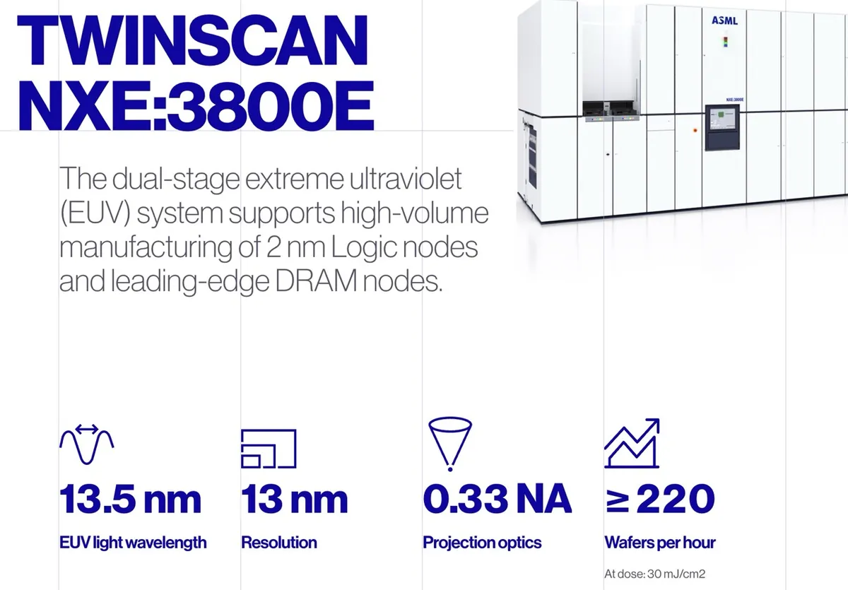
Extreme ultraviolet (EUV) lithography machines generate 13.5 nm light to print sub-2nm microchips. Inside a vacuum chamber, a powerful CO₂ laser strikes microscopic molten tin droplets 50,000 times per second to create light photons /TRUMPF/. Special molybdenum-silicon mirrors reflect and focus this extreme ultraviolet light /Zeiss/. Next-generation High-NA EUV scanners use larger mirror optics to print circuit features down to 8 nanometers in a single exposure /SPIE/.
EUV Laser-Produced Plasma & High-NA Exposure Process
Molten Tin Droplet Injection
50 kHz Droplet StreamFire 50,000 microscopic molten tin droplets per second inside a high-vacuum reaction chamber.
Dual CO₂ Laser Plasma Pulse
13.5nm Light GenerationStrike each tin droplet twice with a 30kW CO₂ laser beam to heat the tin into 13.5nm EUV plasma.
Multilayer Collector Reflection
Bragg Mirror CollectionCollect EUV photons using Carl Zeiss molybdenum-silicon multilayer mirrors under high vacuum.
Vacuum Beam Shaping
High-NA Anamorphic OpticsGuide EUV light beams through 0.55 NA anamorphic mirror optics to shrink circuit images without mask shadowing.
Nanosheet Pattern Exposure
Sub-2nm Transistor PrintingExpose thin photoresist layers on silicon wafers to print sub-2nm nanosheet transistor patterns for AI GPUs.
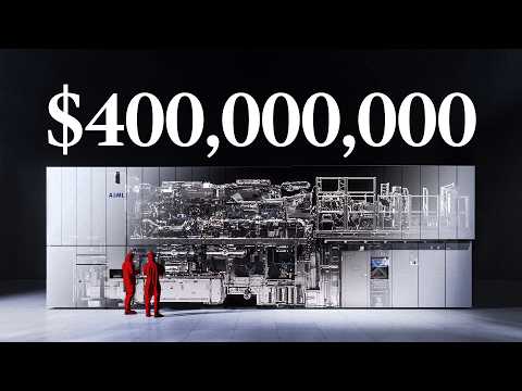
Key technical challenges center on low source power/throughput, stochastic defects, pellicle thermal limits, mask defectivity, and the extreme cost/complexity of High-NA tools (exceeding $350 million per scanner). Because 13.5 nm light is absorbed by virtually all matter, exposures must occur under high vacuum with specialized Mo/Si multilayer reflective mirrors /Zeiss/, where each reflection absorbs ~30% of light. Scaling source power beyond 500–600W, developing durable carbon nanotube (CNT) pellicles, mitigating tin debris via hydrogen buffer gas, and transitioning to metal-oxide resists (MORs) to control stochastic noise and pattern collapse are top priorities.
End-use demand is overwhelmingly driven by AI accelerators, high-performance logic (TSMC N2/A14, Intel 14A/18A), and leading-edge DRAM/HBM (HBM3e/HBM4). Memory revenue is expected to jump sharply in 2026 on HBM and DDR expansions that add more EUV layers /Reuters/; low-NA tools remain the workhorse through at least the late 2020s while high-NA adoption is bifurcated where Intel is already running production-intent silicon /ASML/ while TSMC has deferred high-volume insertion until ~2029 on cost grounds /TrendForce/.
ASML remains the sole volume manufacturer, having delivered 48 EUV systems in 2025 and now targeting at least 60 low-NA units in 2026 with capacity rising ~30% to roughly 85 tools in 2027 (and potentially another 30% toward 110 in 2028) /EETimes/. Lead times remain 18–24 months, constrained by single-source optics. ASML is reportedly weighing value-based price hikes for Low-NA tools tied to productivity gains (e.g., higher WPH on 3800E/F platforms), a move that has frustrated its largest customer (TSMC) /The Information/ which relies heavily on Low-NA systems through at least 2029 and views the increases as undermining its cost-effective multi-patterning strategy.
The technology stack is geopolitically concentrated: ASML (Netherlands) integrates the scanner and holds a 24.9% stake in Carl Zeiss SMT (Germany), which supplies the irreplaceable mirrors, while TRUMPF (Germany) provides the drive lasers /Frontier Map/. All together an EUV lithography system relies on more than 5,100 suppliers with hundreds of sole-source critical parts. Primary users sit in Taiwan, South Korea, and the United States while export controls have blocked EUV sales to China, amplifying both supply-chain fragility and the strategic premium on every tool.
Key Insights
What is the estimated installed base of EUV scanners for leading-edge nodes, and how do next-gen AI architectures like NVIDIA Vera Rubin or AMD Helios rely on them?
ASML’s global cumulative installed base of EUV scanners exceeds 220 active systems, with leading foundries like TSMC and Intel using large fleets, including dozens of NXE:3600/3800 series tools, to scale nodes such as TSMC N2 and Intel 18A. Advanced AI accelerator platforms like NVIDIA’s Vera Rubin and AMD’s Helios rely on these tools to pattern both monolithic 2nm/3nm compute dies and the high-density interposers powering 288 GB HBM4 memory stacks. Because next-generation AI chips pack upwards of 300+ billion transistors, the required EUV exposure layers per wafer are scaling dramatically—often exceeding 15 to 20 EUV mask layers per logic die—making scanner throughput the direct physical ceiling for how many AI accelerators can be produced globally
What is the single most critical bottleneck in EUV process technology today?
The primary process bottleneck centers on source power scaling at the intermediate focus alongside the associated thermal and debris management of the collector mirror. Generating 250 W to 500 W of stable 13.5 nm EUV light requires firing multi-kilowatt CO₂ lasers at 50,000 liquid tin droplets per second; at higher power targets toward 1,000 W, microscopic tin debris rapidly degrades mirror reflectivity unless counteracted by aggressive hydrogen gas buffer flow. Compounding this optical challenge is photon shot noise (stochastic defects) at the wafer level: because 13.5 nm photons carry high energy, fewer photons hit the photoresist per unit dose, forcing an engineering trade-off between power scaling, defect density, and wafer exposure speed.
How do the long-term unit economics, margins, and supply agreements function across the EUV equipment ecosystem?
ASML operates as a sole-source monopoly for EUV systems, generating gross margins in the 50% to 55% range with target long-term gross margins approaching 56% to 60% by 2030. Individual low-NA systems cost around $180M–$200M, while high-NA EXE:5000 tools command upwards of $350M+, backed by multi-year lead times (18–24 months) and long-term supply agreements with leading foundries. This market position is heavily defended by a deeply integrated, highly specialized supply network—such as ASML’s exclusive optical partnership and an equity stake in Carl Zeiss SMT—creating multi-billion dollar barriers to entry and isolating the equipment stack from traditional short-term semiconductor demand cycles.