Photoresists: The Precision Chemicals Powering AI Chip Manufacturing
- David Rogers
- AI Buildout Supply Chain
- 2026-07-15
NEED TO KNOW
- Nanoscale Lithography Chemical: Photoresists combine polymer resins, photoacid generators (PAGs), and specialty solvents (PGMEA) purified to <1–5 ppb metal ions to define sub-5nm features.
- Metal Oxide Resists (MORs) for High-NA EUV: Tin-oxo cluster MORs (pioneered by Inpria/JSR) overcome classic RLS trade-offs and acid diffusion blur in EUV lithography.
- Japanese Supply Chain Hegemony: Japanese suppliers (TOK, JSR, Shin-Etsu) control 70–80% of global photoresist output, creating high geopolitical concentration.
- High Margins & Fab Qualification Barriers: Advanced EUV photoresists command >55% gross margins and high defensibility due to multi-year fab qualification cycles.
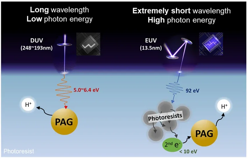
Photoresists are light-sensitive chemical coatings used to print circuit patterns onto semiconductor wafers. Advanced formulations blend polymer resins, light-sensitive acid generators, and high-purity solvents /Semiconductor Engineering/. When exposed to extreme ultraviolet (EUV) light in lithography machines, the chemical coating changes solubility to outline nanoscale transistor features. Chemical suppliers purify photoresists to ultra-low impurity levels to prevent microscopic defects on advanced AI microchips.
EUV Photoresist Lithographic Patterning Process
Spin-Coating Deposition
Uniform Liquid FilmDispense liquid photoresist onto a spinning 300mm silicon wafer to spread a thin, uniform chemical film.
Soft Baking
Solvent EvaporationBake the coated wafer on a hot plate to evaporate solvent liquids and solidify the photoresist layer.
5nm EUV Exposure
Photonic ReactionShine extreme ultraviolet light through a mask onto the photoresist to trigger light-sensitive chemical reactions.
Post-Bake & Wet Development
Pattern UncoveringBake the exposed wafer and wash it with liquid developer chemical to dissolve the exposed resist areas.
Key technical challenges include the resolution-line edge roughness-sensitivity (RLS) tradeoff and stochastic photon noise in EUV, which traditional chemically amplified resists (CARs) struggle with at atomic scales due to acid diffusion blur. Emerging solutions include metal oxide resists (MORs), such as tin-oxo cluster platforms pioneered by Inpria (now JSR) /Microelectronic Engineering/, which offer superior EUV absorption and reduced stochastic noise, helping reduce required doses for higher throughput, lower costs, and fewer defects. Recent advancements in nonalkyl tin oxo clusters show promise for ultrafine resolutions in EUV and electron-beam lithography /Inorganic Chemistry/. Overall, innovations in formulation and processing are actively targeting waste reduction and faster development cycles to support the rapid scaling of AI silicon production.
Global demand for photoresists is surging with the AI boom, as semiconductor capex ramps for logic and HBM chips used in data centers and edge AI. The global market, valued around $4–5 billion recently, is projected to grow at 5–7% CAGR through 2030+, with semiconductors comprising over half and the advanced segment accelerating fastest due to 2nm/High-NA transitions and CHIPS Act-driven fab builds /Mordor Intelligence/. End-uses span AI GPUs/TPUs, smartphones, autos, but AI infrastructure dominates growth narratives.
Supply is highly concentrated and geopolitically sensitive. Japanese companies including Tokyo Ohka Kogyo (TOK), JSR (including Inpria MOR technology), and Shin-Etsu Chemical control approximately 70–80% of global production, especially advanced EUV resists. This dominance creates concentration risk, as demonstrated by the 2019 Japan–Korea export restrictions that threatened memory output and by occasional solvent feedstock disruptions /JT/. While reserves do not apply to synthetic chemicals, fabs maintain buffer inventories. Recycling focuses on solvent recovery from spent streams (decolorization, dehydration, and purification of PGMEA and similar solvents), reducing hazardous waste disposal costs and supporting ESG goals, but formulated resists remain single-use consumables.
Securing resilient photoresist supply chains is therefore as strategically important as the chips themselves for sustained AI progress. Material innovation, solvent circularity, and geographic diversification will determine how quickly and affordably the industry can scale the silicon foundation of the AI era.
Key Insights
What are the estimated volumes of photoresist consumed in manufacturing NVIDIA’s Vera Rubin AI accelerator architecture (or similar leading-edge designs)?
While exact per-unit photoresist volumes for NVIDIA’s Vera Rubin GPUs or platform are not publicly detailed, the architecture’s advanced TSMC 3nm-class nodes, dual-die designs with hundreds of billions of transistors, and extensive EUV lithography steps across numerous mask layers drive substantial consumption of specialized photoresists per wafer.
What is the most critical bottleneck process technology for photoresists in advanced AI accelerator manufacturing like NVIDIA Vera Rubin?
The most critical bottleneck in photoresist technology for advanced AI accelerators like NVIDIA Vera Rubin is the development of EUV and High-NA EUV formulations capable of balancing resolution, line-edge roughness, and sensitivity while minimizing stochastic defects and pattern collapse. Traditional chemically amplified resists struggle at these nodes, necessitating innovations such as metal-oxide resists for improved photon absorption and process windows, with lengthy qualification cycles and supply concentration among Japanese leaders creating ongoing constraints on yield, cost, and throughput in high-volume manufacturing.
What are the unit economics of photoresists, including long-term supply agreements, cyclicality, and margin defensibility?
Photoresist unit economics benefit from long-term supply agreements between Japanese suppliers like TOK, JSR, and Shin-Etsu and major foundries such as TSMC and Samsung, providing volume stability and pricing power amid AI demand, while the market exhibits reduced cyclicality thanks to hyperscale data center investments that sustain growth beyond traditional semiconductor cycles. High gross margins exceeding 55% for advanced EUV variants support margin expansion, with strong defensibility stemming from proprietary chemistry, sub-ppb purity requirements, and multi-year fab qualifications that erect high barriers to entry and favor established players despite geopolitical concentration risks.
What metrology challenges exist for next-generation EUV photoresists, and what market opportunity does this create?
NIST emphasizes the need for advanced in-situ metrology—including real-time Atomic Force Microscopy (AFM) probe methods for monitoring development, soft X-ray spectroscopy and scattering for latent image characterization, and vertical depth profiling—to better quantify and reduce line-edge roughness (LER) and stochastic defects in High-NA EUV photoresists, enabling faster qualification of new formulations and higher yields at sub-10 nm nodes. This creates a substantial market opportunity for metrology equipment providers and specialized service companies, as the EUV photoresist segment is projected to grow at a CAGR exceeding 12% to over $5 billion by 2034, driven by surging demand from AI accelerators on advanced nodes where precise process control directly impacts cost, throughput, and defect reduction.