InP Substrates for Semiconductor Lasers: The Critical Backbone Powering AI Data Centers in 2026
- David Rogers
- AI Buildout Supply Chain
- 2026-07-13
NEED TO KNOW
- Direct Bandgap Telecom Standard: Indium Phosphide (InP) direct bandgap substrates are essential for DFB and EML lasers emitting at 1.3–1.55 µm, the optimal low-attenuation fiber telecom windows.
- Surging Laser Die Density: The shift from 4-channel 400G to 8-channel 800G/1.6T transceivers doubles the required discrete InP laser die count per optical module.
- Severe Substrate Shortages & Investment: Tight supply from leaders Sumitomo, AXT, and JX Advanced Metals is driving major expansions, with JX committing ¥120B to expand capacity 7–10×.
- InP-on-GaAs Cost Reduction: Engineered InP-on-GaAs EpiWafers (developed by Fraunhofer ISE) promise up to 80% cost savings at scale and easier 6-inch+ wafer scaling.
Indium phosphide (InP) substrates are critical materials for high-speed data transmission between AI GPUs. Unlike standard silicon, indium phosphide directly converts electrical signals into laser light with high efficiency /Optica/. This property makes indium phosphide the primary base material for semiconductor lasers and optical integrated circuits. These laser chips generate light signals that travel through fiber optic cables in modern AI data centers.
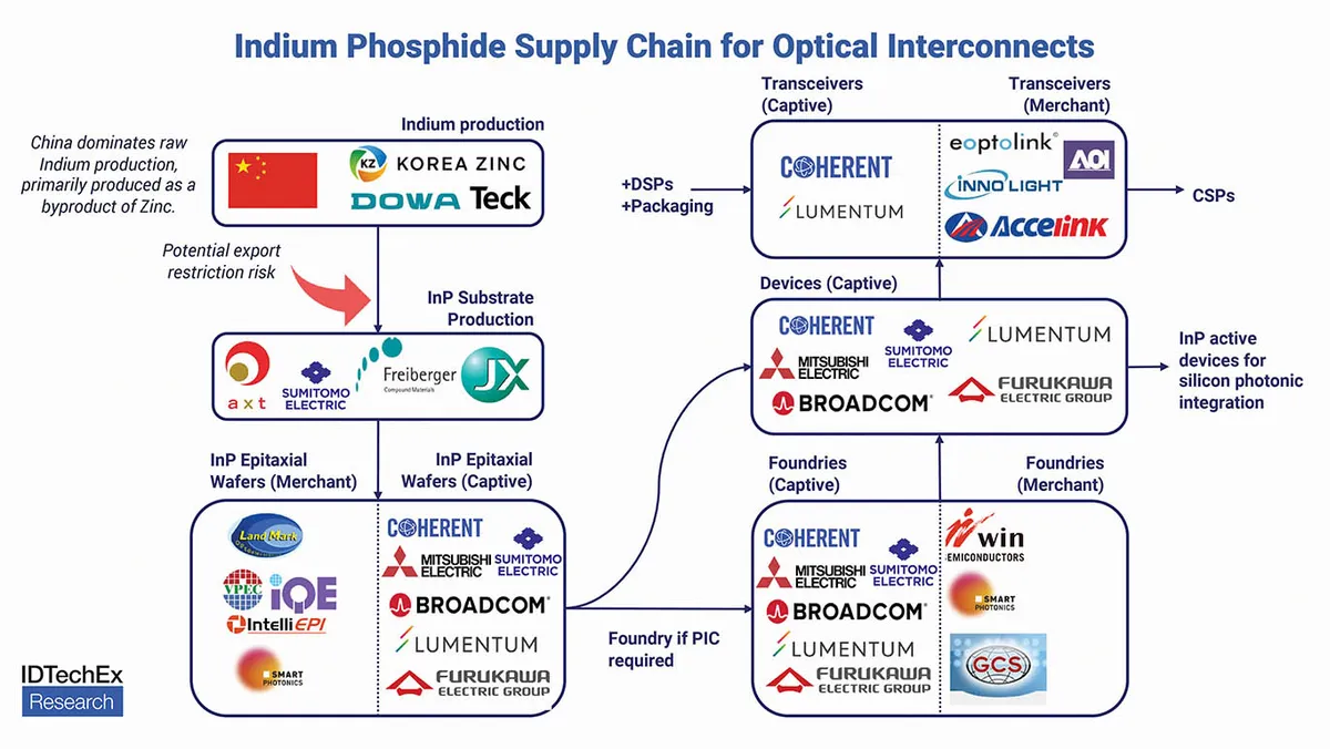
While modern datacenter transceivers utilize a mix of platforms including GaAs-based VCSELs for short-reach links /EI/ and Silicon Photonics (SiPh) for complex optical engines, virtually every single-mode high-speed transceiver relies on an InP (Indium Phosphide) laser source to generate the primary optical carrier wave. As hyperscalers rapidly transition to 800G and 1.6T architectures, demand for high-speed InP laser dies is surging; the shift to parallel optical lanes (such as moving from 4-channel 400G to 8-channel 800G/1.6T) effectively doubles the discrete laser die count required per transceiver module /IEEE/.
InP Laser Substrate & Transceiver Manufacturing Process
High-Purity InP Synthesis
Polycrystalline Alloy ProductionReact pure 6N indium metal with purified phosphorus gas under high pressure to synthesize InP material.
VGF Single-Crystal Growth
Low-Defect Ingot PullingGrow single-crystal InP boules using Vertical Gradient Freeze furnaces to keep crystal defect density extremely low.
Wafer Slicing & CMP Polishing
Substrate Surface PreparationSlice InP boules into 6-inch wafers and polish them to sub-nanometer flatness.
MOCVD Active Layer Epitaxy
Quantum Well DepositionDeposit thin semiconductor layers on the wafer using MOCVD to create laser light-emitting quantum wells.
Laser Cleaving & Module Integration
Optical Transceiver PackagingEtch laser mirrors, dice the wafer into discrete laser dies, and mount them into 1.6T optical transceivers for AI GPU links.
Yet 2026 has brought a stark reality: severe InP substrate shortages /Yole/. Supply is highly concentrated (top players like Sumitomo Electric, AXT, and JX Advanced Metals dominate), lead times are long, and geopolitical export controls have tightened availability. Prices have climbed sharply, and new capacity takes years to qualify and ramp.
Alternative compound semiconductor engineered substrates such as thin InP layers on larger, lower-cost GaAs wafers (InP-on-GaAs) are delivering comparable device performance with dramatically lower cost potential (up to 80% savings at scale) and better scalability to 6-inch+ formats. Fraunhofer ISE and partners have already demonstrated InP-on-GaAs or kerfless epitaxial silicon (EpiWafers) wafers with excellent uniformity and low defect densities /AIP/. Major suppliers are also investing aggressively as JX Advanced Metals alone committed up to ¥120 billion (~$800M) over four years to expand capacity 7-10× specifically for AI-driven optical communications demand /JX/.
Despite these challenges and promising alternatives, Indium Phosphide continues to underpin the optical interconnects essential for AI scaling /NVIDIA/. Continued investment in both traditional substrate capacity and engineered solutions will be critical to meeting the explosive demand for high-speed lasers. The race to secure reliable InP supply may well define the pace of next-generation data center deployments through the end of the decade.
Key Insights
Why can’t copper handle interconnects when 576 GPUs span eight racks in systems like NVIDIA Vera Rubin Ultra NVL576?
When 576 GPUs span eight racks and operate as a single system — as they will in NVIDIA Vera Rubin Ultra NVL576, which links eight NVLink racks of 72 NVIDIA Rubin Ultra GPUs into one 576-GPU domain — copper can’t carry the signal across that distance. High-bandwidth, low-latency optical interconnects powered by InP-based lasers become mandatory to keep the entire domain coherent. This multi-rack scaling is a primary driver of surging demand for InP substrates used in the laser sources of next-generation AI optical engines.
What makes InP substrates the preferred platform for high-performance semiconductor lasers in AI data centers?
InP’s direct bandgap enables efficient generation of coherent laser light at the exact telecom wavelengths (1.3–1.55 μm) where optical fiber attenuation is lowest, unlike silicon. This allows fabrication of advanced DFB, electro-absorption modulated, and tunable lasers plus full monolithic photonic integrated circuits that combine lasers, SOAs, modulators, and photodetectors on one chip. Virtually every single-mode high-speed transceiver (800G/1.6T and beyond) relies on an InP laser source as the primary optical carrier.
How are InP substrate shortages and new engineered alternatives impacting AI infrastructure scaling in 2026?
Severe InP substrate shortages, concentrated supply among a few players (Sumitomo Electric, AXT, JX Advanced Metals), long lead times, and geopolitical export controls have driven sharp price increases and constrained laser die availability. Engineered solutions such as InP-on-GaAs wafers offer comparable performance, up to ~80% cost savings at scale, and easier scaling to 6-inch+ formats, while major suppliers are investing heavily (e.g., JX’s ¥120 billion capacity expansion). Resolving this bottleneck is now a critical path item for next-generation multi-rack AI systems.