Inside the Package Optical Engine: Architecture, Packaging, and Physical Limits
- David Rogers
- AI Buildout Supply Chain
- 2026-09-02
NEED TO KNOW
- Overcoming Copper Reach Limits: High-speed serialized electrical signaling (224 Gbps PAM4) faces severe dielectric attenuation beyond 1 to 2 meters; co-packaged optics (CPO) shrink on-package copper traces to microns before converting signals to light over single-mode fiber.
- Ultra-Low Energy and Latency: Direct-drive optical engines reduce interconnect energy consumption to a few picojoules per bit by eliminating power-hungry DSP retimers, simultaneously removing tens of nanoseconds of latency per hop.
- Thermal Isolation Strategy: Because InP laser diode failure rates accelerate exponentially under high junction temperatures, continuous-wave (CW) lasers are decoupled into external pluggable modules rather than remaining on hot kilowatt-class accelerator packages.
- Active Thermal Management: Silicon micro-ring modulators experience a thermo-optic drift of approximately 70 to 80 pm/°C, requiring direct-to-chip liquid cooling and dedicated closed-loop micro-heaters to maintain optical resonance.
- Packaging and Assembly Bottlenecks: Sub-micron fiber-to-waveguide alignment tolerances (±0.2 to 0.5 µm) mandate automated active-alignment tooling over manual assembly, while multi-die heterogeneous bonding exacerbates substrate warpage and compound yield loss.
- Supply Chain and Geopolitical Choke Points: Commercial volume is constrained by 300 mm photonic wafer starts, advanced 2.5D/3D packaging lines (predominantly in Taiwan), and refined indium supplies, where Chinese export controls impact the single-crystal InP substrate market.
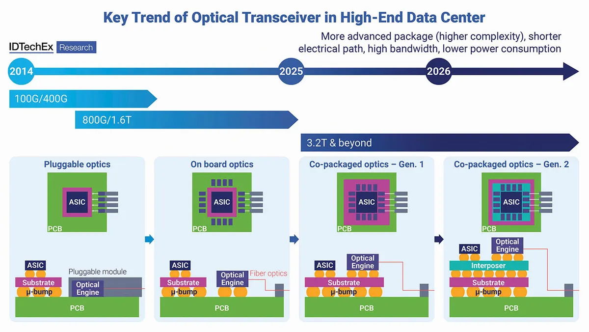
Package optical engines are the fundamental physical converters powering next-generation optical I/O. As data rates climb to 200 Gbps per lane and beyond, electrical signals degrade rapidly, requiring dedicated optical engines to translate high-speed electron streams into photons directly at the engine boundary. The core of every engine is a tightly coupled heterogeneous pair: a photonic integrated circuit (PIC) and an electronic integrated circuit (EIC). The EIC provides analog drive currents and transimpedance amplification (TIA), operating just microns away from the PIC’s optical components.
Manufacture is a multi-material semiconductor stack: CMOS-compatible silicon photonics patterned on 300 mm wafers (routing optical waveguides, micro-ring modulators, and epitaxial germanium photodetectors), direct vertical 3D or micro-bump integration (such as copper-to-copper hybrid bonding of the EIC directly over the PIC), and precision fiber-array units (FAUs). High-power continuous-wave (CW) indium phosphide (InP) lasers supply the raw optical carrier power, but they are deliberately isolated from the engine core to preserve laser diode reliability /Leonardo/. Fabricating these engines demands sub-nanometer foundry process discipline, because waveguide propagation loss and modulator optical resonance are far less tolerant of sidewall roughness than standard digital CMOS logic.
The core engineering bottlenecks within the engine are physical alignment, local thermal drift, and assembly yield. Coupling incoming and outgoing light between arrays of single-mode fibers and on-chip waveguides requires mechanical alignment precision down to a few tenths of a micron; manual assembly is fundamentally too slow, making automated sub-micron machine-vision packaging indispensable. Thermal stability presents an internal operational challenge: silicon micro-ring modulators drift optical resonance by roughly 70 to 80 pm/°C, meaning temperature fluctuations quickly knock channels out of alignment unless active integrated micro-heaters and closed-loop phase tuning are built directly into the engine layout. Furthermore, combining separate PIC and EIC dies into a single functional unit multiplies compound yield loss and introduces mechanical warpage across the micro-interposer. The industry is resolving these internal constraints with blind-mate, detachable optical connectors for serviceability, dense hybrid bonding to maximize bump pitch density, and dense wavelength-division multiplexing (DWDM) to multiply data channels per optical path. Open technical consortiums such as the /CW-WDM MSA/ and /OIF/ are standardizing engine electrical interfaces and multi-wavelength laser profiles so optical engines can scale throughput from 200 Gbps per fiber up toward 800 Gbps while avoiding proprietary PHY architectures.
The primary role of the optical engine is raw data conversion at ultra-low energy and extreme throughput. By handling signal amplification and electro-optic conversion in direct proximity, the engine eliminates heavy digital signal processors (DSPs), slashing power consumption down to a few picojoules per bit and removing serialization latency. Engine-level aggregate bandwidth targets already range from 1.6 Tbps to 6.4 Tbps per unit /Skorpios/, with modular designs tiling multiple engines to supply dozens of terabits of optical escape bandwidth across a compact footprint. As high-speed transmission pushes past standard copper tolerances, the package optical engine stands as the critical, self-contained sub-system bridging high-performance silicon to high-density fiber-optic fabrics.
Key Insights
What is the internal architecture of an in-package optical engine, and how does it achieve ultra-low energy and latency?
A package optical engine consists of a tightly coupled heterogeneous stack combining a Photonic Integrated Circuit (PIC) and an Electronic Integrated Circuit (EIC). The EIC provides analog driver currents and transimpedance amplification (TIA) placed just microns away from the PIC's silicon optical components via 3D copper-to-copper hybrid bonding or fine-pitch micro-bumps. By placing analog drive electronics in extreme proximity to silicon modulators (such as micro-ring or Mach-Zehnder modulators) and germanium photodetectors, the engine eliminates heavy, power-hungry Digital Signal Processors (DSPs) and SerDes retimers. This direct-drive architecture slashes interconnect energy consumption down to a few picojoules per bit (pJ/bit) while eliminating tens of nanoseconds of serialization latency per link hop.
Why are Continuous-Wave (CW) InP lasers decoupled into external modules rather than integrated directly on the optical engine?
Indium Phosphide (InP) continuous-wave (CW) lasers are thermally decoupled into external pluggable laser sources (ELS) because laser diode failure rates accelerate exponentially with elevated junction temperatures (governed by Arrhenius activation kinetics). Placing sensitive multi-wavelength direct-bandgap lasers directly on or adjacent to kilowatt-class AI accelerator or switch packages operating at 85°C to 105°C+ causes rapid threshold current degradation, optical power drop-off, and reduced mean time between failures (MTBF). Decoupling CW lasers into serviceable, field-replaceable external modules operating at lower ambient temperatures with dedicated thermoelectric coolers (TECs) preserves laser longevity and allows independent laser replacement without discarding expensive host compute/switch ASICs.
What are the primary packaging and physical alignment bottlenecks in manufacturing high-density optical engines?
The foremost manufacturing bottlenecks are sub-micron optical fiber-to-waveguide alignment, thermo-optic resonance drift, and multi-die substrate warpage. Coupling single-mode optical fibers to on-chip sub-micron silicon waveguides mandates sub-micron alignment tolerances (±0.2 to 0.5 µm), requiring automated active machine-vision alignment tooling during fiber-array unit (FAU) packaging. Operationally, silicon micro-ring modulators exhibit a thermo-optic drift of approximately 70 to 80 pm/°C, necessitating dedicated integrated micro-heaters and closed-loop control circuitry to lock resonance wavelengths. Furthermore, heterogeneous 3D hybrid bonding between EIC, PIC, and micro-interposers compounds assembly yield loss and introduces mechanical warpage across thermal cycles, making advanced wafer-level packaging capacity and precision test infrastructure critical industry bottlenecks.
What are the unit economics, margin structures, and commercial scaling dynamics for optical engine suppliers?
Optical engine economics are governed by high-margin, sticky manufacturing and packaging agreements rather than cyclical commodity transceiver dynamics. Tier-one suppliers secure defensible gross margins of 45% to 60% through multi-year Long-Term Supply Agreements (LTSAs) and take-or-pay volume commitments with hyperscalers and primary silicon designers. While Non-Recurring Engineering (NRE) costs and precision packaging tooling investments are significant, high switching costs, custom Process Design Kits (PDKs), and stringent qualification hurdles create strong competitive moats. As manufacturing scales from 1.6 Tbps to 6.4 Tbps+ engines per socket and packaging yields mature, supplier revenue expansion is driven by increasing optical content per AI compute tray and switch chassis rather than unit price inflation.