Co-Packaged Optics and the Industrial Bottlenecks of Rack-Scale AI Interconnects
- David Rogers
- AI Buildout Supply Chain
- 2026-09-01
NEED TO KNOW
- Core Architecture: Co-packaged optics (CPO) collapses electrical SerDes traces from centimeters to millimeters by hybrid-bonding electronic and photonic dies directly onto advanced substrates (e.g., TSMC COUPE, GF Fotonix).
- Physical & Thermal Hurdles: The primary bottlenecks are mechanical and thermal rather than lithographic, requiring sub-micron fiber alignment (±0.5–1 µm), tolerance to 260 °C solder reflow, and protection against microring resonance drift near kilowatt-class ASICs.
- Laser Dependency: Because silicon cannot efficiently emit light, optical engines rely on external 300–400 mW Indium Phosphide (InP) continuous-wave (CW) lasers with dedicated thermoelectric cooling.
- Adoption Roadmap: Switch-side CPO (Broadcom Tomahawk 5, NVIDIA Quantum-X/Spectrum-X) ships in the 2025–2026 window, while compute-side optical I/O replacing copper scale-up fabrics (like NVLink across 576–1,024+ GPUs) is targeted for 2028.
- Supply Chain Chokepoints: Manufacturing scaling is constrained by specialized InP laser epitaxy capacity and raw substrate suppliers (Sumitomo, AXT, Yunnan Germanium) rather than standard silicon CMOS wafer output.
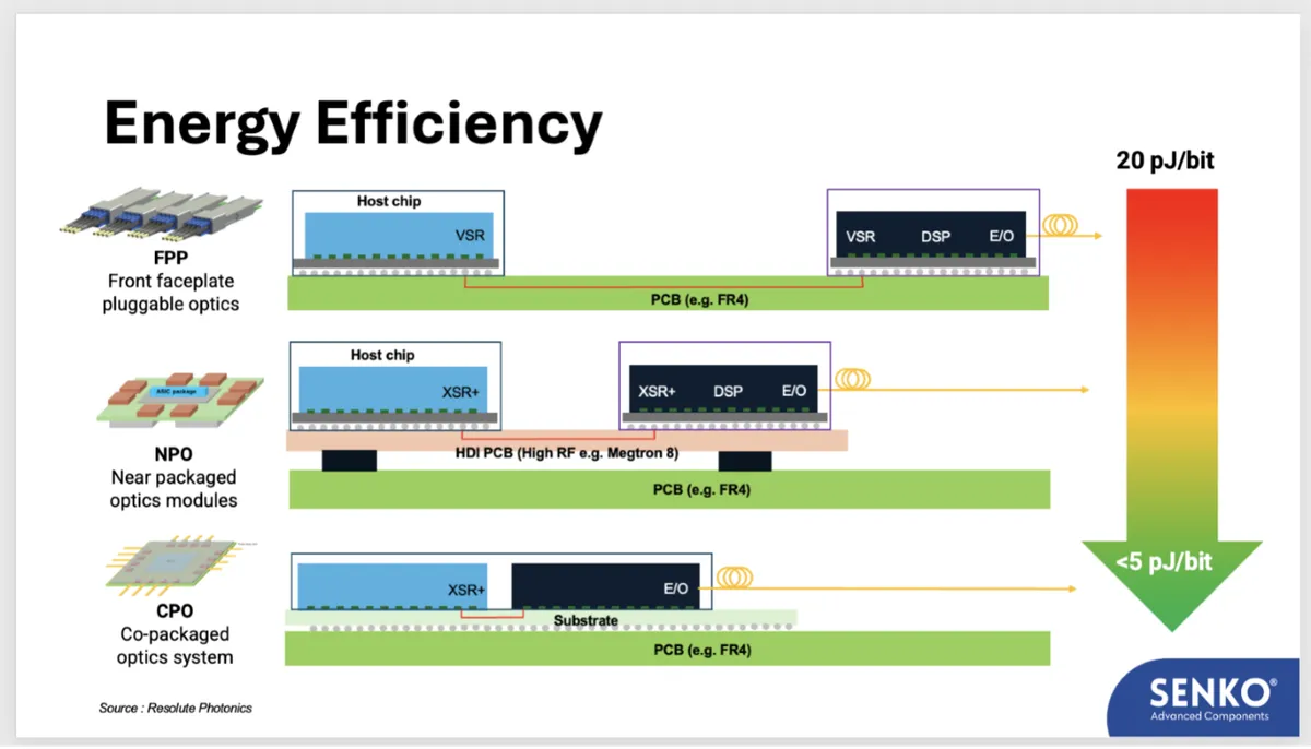
Co-packaged optics (CPO) for rack-scale chip-to-chip links is not a simple transceiver refresh. It is a foundry and packaging challenge. In this design, a photonic integrated circuit (PIC) and an electronic integrated circuit (EIC) connect millimeters away from a switch or accelerator die. This short distance collapses electrical traces from centimeters to millimeters before light leaves the package through a fiber array. TSMC’s COUPE platform stacks the electronic die onto the photonic die using SoIC-X hybrid bonding and places that engine onto a CoWoS substrate /Semiconductor Engineering/. GlobalFoundries’ Fotonix platform fabricates photonics and control electronics together on the same 45 nm wafer /IEEE/. Because silicon cannot emit light efficiently, an off-package indium phosphide (InP) continuous-wave (CW) laser powers each engine. This hybrid structure of silicon-based PICs paired with compound-semiconductor light sources is the core manufacturing capability that modern AI server racks require.
| Feature | Pluggable Optics (~100+ mm away) | Co-Packaged Optics (~1–10 mm away) |
|---|---|---|
| Power Consumption | High (requires heavy equalization to fight PCB trace loss) | Very Low (minimal signal degradation over millimeters) |
| Bandwidth Density | Limited by edge panel space | Extremely High (escapes the ASIC via high-density optical fibers) |
| Latency | Higher (due to processing and distance) | Ultra-Low |
The primary engineering challenges are mechanical and thermal rather than lithographic. A single-mode fiber core is approximately 9 µm wide, while a silicon waveguide is only hundreds of nanometers wide. Fiber-array units (FAUs) must align tens to 160 fibers within a ±0.5–1 µm tolerance. These units must survive 260 °C solder reflow temperatures and operate next to kilowatt-class ASICs whose heat shifts optical resonances and warps the package substrate. High-power continuous-wave lasers for CPO must deliver roughly 300–400 mW, compared to 70–100 mW in a standard pluggable optical module. Engineers place these lasers off-die with thermoelectric coolers because temperature changes from the processor shift the laser wavelength and degrade performance. Standardized wafer-level testing, detachable optical connectors, and multi-die assembly yields remain immature. Assembly and test providers note that a lack of industry standards keeps multi-vendor compute-side CPO 12 to 24 months away from high-volume delivery /Semiconductor Engineering/.
The optical link budget and total energy efficiency of co-packaged optical interconnects are modeled as:
Market adoption follows two distinct timelines. Switch-side CPO is already shipping in initial systems: Broadcom’s Tomahawk 5-Bailly (51.2 Tbps Ethernet) and NVIDIA’s Quantum-X photonics switch operate in the 2025–2026 window, with Spectrum-X photonics and 102–410 Tbps systems scheduled for late 2026. Compute-side optical I/O, the direct chip-to-chip fabric intended to replace copper NVLink cables across 576 to 1,024+ accelerators, will arrive later. NVIDIA plans compute-level optical NVLink around 2028, alongside merchant solutions from Ayar Labs (TeraPHY with SuperNova lasers), Celestial AI with Marvell, and Intel. Industry forecasts range from $100–200 million currently to projections reaching >$20 billion by 2030 if scale-up compute fabrics adopt optics widely /TrendForce/. Hyperscale cloud operators (such as Meta, Microsoft, Oracle, CoreWeave, and Lambda) represent the first deployment targets.

Manufacturing capacity is constrained by photonics fabrication lines and laser production rather than standard logic wafer volume. Industry estimates place TSMC’s PIC production at approximately 500 wafers per month recently, scaling toward 10,000 in early 2026, 15,000 by late 2026, and 25,000 by 2028 /Commercial Times/. After accounting for packaging and test yields, this volume supports tens of millions of optical engines only toward the end of the decade. The tighter bottleneck is InP laser production. Laser manufacturers report that output trails customer demand by more than 30%, high-power component qualification remains difficult, and major chipmakers have committed billions of dollars in multi-year agreements to secure factory lines. Raw substrate supply is concentrated among a few suppliers, including Sumitomo Electric, AXT, and Yunnan Germanium /EI/. Because these integrated modules are complex and low in physical volume compared to copper or memory, mature recycling and recovery processes do not yet exist.
| Category | Primary Entities | Key Technical Metric / Physics Parameter | Status / Validation |
|---|---|---|---|
| Packaging & Foundry | TSMC, GlobalFoundries | SoIC-X 3D Hybrid Bonding, CoWoS, 45 nm RF SOI | Validated; sub-millimeter SerDes trace collapse. |
| Optical Alignment | Corning, FOCI, SENKO | Core MFD: 9 µm to Si waveguide: 450 nm; ±0.5 µm tolerance | Validated; mechanical CTE & solder reflow limits. |
| Laser Sources | Lumentum, Coherent | InP direct bandgap; 300–400 mW CW output; thermo-optic ~0.1 nm/°C | Validated; $2B multi-year capacity lock-ins. |
| Substrates | Sumitomo, AXT, Yunnan Ge | Direct crystal InP growth (VGF/LEC) | Validated; critical upstream raw-material choke. |
| Deployment Roadmaps | Broadcom, NVIDIA | 51.2T switch CPO (2025–26) → NVLink CPO (>576 GPUs, ~2028) | Validated; switch optics precedes compute I/O. |
The supply chain relies on a concentrated global manufacturing network. NVIDIA and Broadcom define the system architectures; TSMC provides high-volume PIC fabrication and advanced packaging; GlobalFoundries provides a merchant silicon photonics alternative in the United States; Lumentum and Coherent manufacture high-power lasers; and suppliers such as FOCI, Corning, SENKO, Molex, TE Connectivity, and Sumitomo supply precision fiber arrays and connectors. This creates a geographically distributed dependency: advanced packaging in Taiwan, laser fabrication in the United States and Japan, and raw substrate materials partly sourced from China. A disruption at any single step of photonic wafer output, laser yield, or optical alignment tooling will not stop standard processor fabrication, but it will restrict the optical bandwidth needed to link those processors into unified, rack-scale computing clusters.
Key Insights
What is the projected volume and install-base attach rate of optical engines in rack-scale AI architectures like NVIDIA Vera Rubin NVL72 and AMD Helios?
Rack-scale AI architectures are transitioning from copper backplanes to optical fabrics as interconnect bandwidth scales past 200 Gbps per lane, driving a multi-million-unit optical engine market. In a 72-accelerator liquid-cooled domain (such as NVIDIA NVL72 or prospective Vera Rubin configurations), a full optical scale-up switch-to-compute topology requires between 8 to 16 optical engines per compute tray and 8 to 32 optical engines per switch ASIC (e.g., 512-lane 200G Spectrum-X or Quantum-X photonics), generating an attach density of roughly 500 to over 1,000 optical engines per rack. At hyperscaler deployment volumes spanning hundreds of thousands of accelerators, annual optical engine shipments will scale from pilot volumes of roughly 500,000 units in the 2025–2026 switch-first era to tens of millions of units annually by 2028–2030 as compute-side optical I/O replaces passive copper DAC cables in clusters exceeding 576 to 1,024+ XPUs.
What is the most critical process technology bottleneck limiting co-packaged optics scaling?
The most critical bottleneck is the epitaxy yield and high-power operational stability of external Indium Phosphide (InP) continuous-wave (CW) lasers, compounded by sub-micron fiber-array unit (FAU) packaging. Because indirect-bandgap silicon cannot generate light, each optical engine requires an external InP direct-bandgap source outputting 300–400 mW of unmodulated optical power to overcome insertion, splitter, and coupling losses. Manufacturing high-power CW InP lasers with strict single-mode wavelength stability across thermal gradients is constrained by 3-inch/4-inch wafer crystal growth limits and defect densities. Downstream, packaging tools must actively align 64 to 160 optical fibers to silicon waveguides within a ±0.5 µm spatial tolerance while ensuring the optical assembly survives 260 °C solder reflow and package warpage from adjacent kilowatt-class ASICs.
What are the unit economics, margin structures, and supply-agreement dynamics governing CPO components?
CPO component unit economics are shifting from low-margin transceiver commodity cycles toward sticky, high-margin advanced packaging and proprietary compound-semiconductor supply agreements. Because optical engine failure destroys the entire multi-thousand-dollar host ASIC/CoWoS package, hyperscalers and chipmakers avoid spot markets and instead secure multi-year, multi-billion-dollar Long-Term Supply Agreements (LTSAs) with non-recurring engineering (NRE) prepayments to lock InP laser and advanced packaging capacity. This structural shift provides strong gross margin defensibility (exceeding 50–60% for specialized laser epitaxy and precision packaging) and shields optical component makers from historical telecom inventory cyclicality, as optical demand becomes directly tied to multi-year data-center capital expenditure cycles.