Inside NVLink Rack Fabrics: Why Copper Still Dominates AI Scale-Up Over Optics
- David Rogers
- AI Buildout Supply Chain
- 2026-08-31
NEED TO KNOW
- Rack-Scale Shared Memory: NVLink Switch ASICs unify up to 72 GPUs into a single coherent memory domain, delivering up to 3.6 TB/s per GPU and 260 TB/s of aggregate bisection bandwidth across NVL72 racks.
- Direct Copper Dominance: High-density twinaxial flyover cables and blind-mate connectors (Amphenol Paladin) bypass lossy PCB traces at 224 Gbps PAM4 (56 GHz Nyquist), maintaining electrical signal integrity 5–10x cheaper per bit than optics.
- In-Network Computation: Hardware-based SHARP engines offload all-to-all collective reductions into switch silicon, eliminating communication overhead on GPU tensor cores.
- The 1-Meter Reach Wall: Insertion loss at 200–400G per pair restricts passive copper to ~1 meter, establishing the physical boundary where multi-rack scale-up fabrics must transition to Co-Packaged Optics (CPO) and hybrid bonding (TSMC COUPE).
- Packaging & Silicon Bottlenecks: Primary supply chokepoints center on reticle-sized 800 mm² switch ASICs, TSMC CoWoS packaging, precision 224G connector micro-welding, and continuous-wave laser foundries.
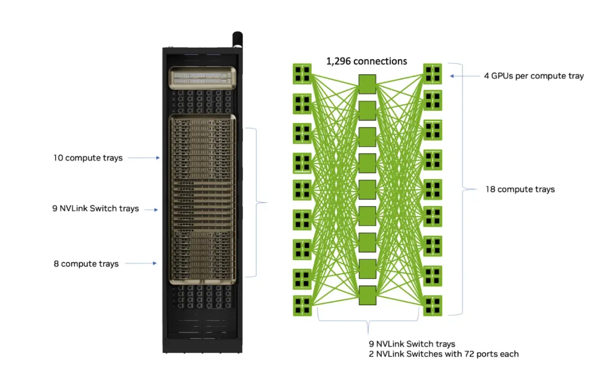
NVLink-style rack fabrics serve as the core interconnect that unifies dozens of discrete accelerators into a single shared-memory computer /NVIDIA/. In NVIDIA’s NVL72-class systems, fifth- and sixth-generation NVLink protocols combine with dedicated NVLink Switch ASICs to build an all-to-all network /NVIDIA/. Across this fabric, 72 GPUs transfer memory traffic at 1.8 to 3.6 TB/s per accelerator, delivering 130 to 260 TB/s of aggregate bandwidth across the rack. Hardware-based reduction engines (SHARP) execute mathematical operations directly inside switch silicon, preventing communication bottlenecks on GPU compute cores. The physical interconnect inside the rack relies almost entirely on copper /IEEE/: thousands of 200 Gb/s PAM4 differential pairs, high-density Amphenol Paladin connectors, and low-loss twinaxial cables. Direct flyover cables bypass printed circuit board (PCB) traces entirely because dielectric losses and crosstalk at 56 GHz Nyquist frequencies degrade signals over standard circuit boards. At the package level, NVLink-C2C links compute dies over silicon interposers with low-power PHYs (< 1 pJ/bit), while the NVLink Fusion architecture licenses this stack so custom XPUs can attach via UCIe bridge chiplets. To eliminate memory-access bottlenecks within the package, Fusion now integrates NVHBM, a custom base-die design that moves the memory controller directly into the 3D HBM stack /NVIDIA/, cutting PHY area by up to 67%, reducing memory power by 15%, and delivering up to 30% more memory bandwidth than standard HBM4e.

The aggregate bisection bandwidth and physical energy limits of scale-up domains are modeled as:
The primary engineering challenge is the silicon and electro-mechanical assembly rather than the raw wire. Each NVLink Switch ASIC is a maximum-size, reticle-limited die measuring over 800 mm² with roughly 50 billion transistors, manufactured on TSMC’s customized 4N/4NP process. A substantial portion of the die area is dedicated to high-speed SerDes physical layers that share design blocks with Quantum InfiniBand and Spectrum Ethernet switches. Fabricating these switches demands the same advanced packaging (such as TSMC CoWoS), power delivery, and thermal solutions required by leading-edge GPUs. Mechanically, the rack spine operates as a floating, precision-aligned system: trace length variation, high-frequency signal attenuation, and blind-mate mechanical tolerances (±3 mm float) represent strict manufacturing limits. Manufacturing costs concentrate in precision termination, automated paddle-card micro-welding, and multi-pin connectors rather than bulk copper. Within a single rack frame, passive copper remains roughly five to ten times cheaper per bit than optical transceivers /NVIDIA/, which is why scale-up interconnects remain electrical while scale-out fabrics transition to fiber.
Physical constraints in copper transmission define the next scaling boundary. At 200 to 400 Gb/s per differential pair, insertion loss limits passive copper reach to approximately one meter. Expanding the scale-up domain beyond a single rack frame requires either complex mechanical packaging or a transition to co-packaged optics (CPO). Technologies such as direct 3D hybrid bonding of electronic and photonic dies (like TSMC COUPE), external laser sources (ELS), and optical engines from ecosystem partners like Ayar Labs and Lightmatter reduce power consumption and package trace lengths. However, optical systems introduce distinct reliability risks, including laser sensitivity to high operating temperatures on 1 kW+ packages, continuous laser degradation, and sub-micron fiber alignment requirements during assembly. Open scale-up standards like UALink and Ultra Ethernet aim to provide multi-vendor alternatives for this accelerator tier /Business Wire/, with native switch silicon sampling across the industry between 2025 and 2027.
| Fabric / Architecture | Primary Backer | Ecosystem Type | Scope / Scale | Primary Physical Medium |
|---|---|---|---|---|
| NVLink / NVLink Switch | NVIDIA | Proprietary / Licensed via Fusion | Up to 72 (NVL72 copper) or 576+ (Optics) | 224G Copper Twinax / CPO |
| Infinity Fabric (xGMI) | AMD | Proprietary | 8 GPUs per node | PCB / OAM Baseboard |
| UALink | AMD, Broadcom, Intel, Meta, Google | Open Standard | Up to 1,024 Accelerators | 224G Copper / Optical |
| ICI + OCS | Proprietary (Internal Cloud) | Up to 4,096+ TPUs | Reconfigurable Fiber / MEMS Optics | |
| NeuronLink | AWS | Proprietary (Internal Cloud) | Up to 64–128+ Trainium chips | Chassis Midplane / Copper |
| Scale-Up Ethernet (UEC) | Broadcom, Arista, Cisco, AMD | Open Standard | Cluster / Multi-Rack | Copper DAC / Optical Transceivers |
Interconnect demand is driven primarily by distributed AI workloads rather than traditional host networking. Mixture-of-Experts (MoE) architectures, key-value (KV) cache sharing across distributed nodes, and tensor-parallel execution models require intra-domain bandwidth to expand faster than standard scale-out networks. High-density scale-up networking represents the fastest-growing segment of data-center hardware, generating billions of dollars in specialized switch and backplane content per generation. Rather than forcing custom chips into isolated silos, hyperscalers and custom silicon designers are increasingly adopting NVLink Fusion; AWS is integrating Trainium4 into NVIDIA’s MGX rack architecture /NVIDIA/, while MediaTek adopted NVLink Fusion backed by a $3.5 billion NVIDIA convertible bond investment to give custom XPU developers a prevalidated route to NVLink-connected AI factories /NVIDIA Newsroom/. Over the long term, scaling coherent memory domains to optical multi-rack clusters (spanning 576 to 1,152+ accelerators) will become standard once physical rack space and copper reach limits are exhausted.
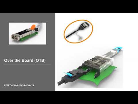
Supply capacity is constrained by advanced lithography, packaging, and precision electro-mechanical tooling rather than raw materials. Switch and accelerator silicon production concentrates heavily on advanced TSMC process nodes and Taiwan-based CoWoS packaging lines /EI/, even as wafer fabrication expands into regional facilities. High-speed connector components and internal flyover cable harnesses rely on specialized manufacturers like /Amphenol/, TE Connectivity, and /Samtec/. Meanwhile, silicon photonics capacity and continuous-wave laser manufacturing remain concentrated among specialized III-V foundries and photonics providers. While copper harnesses are easily separated and recycled at end-of-life, multi-chip semiconductor packages and photonic engines present complex composite materials that are difficult to reclaim. The critical strategic risk remains centered on leading-edge packaging lines, proprietary interconnect IP, and the few manufacturing facilities capable of producing 224G connectors and co-packaged optical assemblies at scale.
Key Insights
How does NVLink achieve unified shared memory across a rack?
NVLink-style rack fabrics use dedicated NVLink Switch ASICs to connect dozens of accelerators (e.g., 72 GPUs in NVL72) into a single, memory-mapped domain providing 1.8 to 3.6 TB/s per GPU and up to 260 TB/s of aggregate rack bandwidth.
What is in-network computation in NVLink fabrics?
Hardware-level aggregation engines (such as SHARP) perform reduction operations directly inside the switch silicon, freeing GPU compute cores from communication bottlenecks.
Why does passive copper dominate intra-rack scale-up interconnects?
High-frequency signaling at 224 Gbps PAM4 avoids printed circuit board (PCB) traces by using direct twinaxial flyover cables and high-density blind-mate connectors (such as Amphenol Paladin) to maintain signal integrity at 56 GHz Nyquist frequencies. Intra-rack passive copper is also 5 to 10 times less expensive per bit than optical transceivers.
What is the physical reach limit for passive copper interconnects?
As per-lane data rates hit 200–400 Gbps, passive copper reaches an insertion loss wall at roughly 1 meter, forcing multi-rack scale-up architectures to eventually transition to Co-Packaged Optics (CPO) and hybrid-bonded electronic-photonic packaging (like TSMC COUPE).
Where are the primary supply chain bottlenecks in scale-up interconnects?
Manufacturing limits stem from advanced packaging capacity (such as TSMC CoWoS), precision connector micro-welding, and specialized III-V semiconductor laser foundries rather than raw commodity materials.
How does the NVIDIA and MediaTek partnership expand NVLink Fusion?
MediaTek adopted the NVLink Fusion platform backed by a $3.5 billion NVIDIA investment to provide a prevalidated foundation for custom multi-die XPUs, combining MediaTek's SoC design and custom silicon capabilities with NVLink scale-up connectivity, NVLink-C2C, and NVHBM memory architectures.