Glass Core Substrates & Interposers: The Future of AI Chip Packaging
- David Rogers
- AI Buildout Supply Chain
- 2026-08-13
NEED TO KNOW
- Performance & Scaling Jump: Glass core substrates and interposers replace organic (ABF) cores and silicon interposers, matching silicon's thermal expansion (~3 ppm/°C) to enable packages over 70–100 mm per side with minimal warpage and up to 10× higher interconnect density.
- Superior Electrical Properties: Ultra-flat glass surfaces feature low dielectric loss (tan δ ≈ 0.001–0.003) and support fine line/space features down to ~2/2 µm, delivering lower signal loss and improved power delivery for HBM and chiplet architectures.
- Manufacturing Hurdles: Glass brittleness, via sidewall roughness, metal adhesion, and high-aspect-ratio copper voiding keep panel handling yields in the 70–85% range, lagging behind mature organic substrates (>90%) and driving up initial production costs.
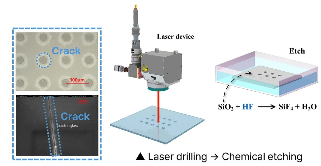
- Laser-Induced Via Fabrication: Process refinements rely on Laser-Induced Deep Etching (LIDE) to form Through-Glass Vias (TGVs) without micro-cracking, alongside specialized pulse-plating chemistry and edge-protection tooling to improve panel-scale yields.
- Market Growth & Timelines: Driven by AI accelerators and co-packaged optics, the glass substrate and fan-out panel-level packaging market is projected to grow from ~650 million in 2024 to over 8 billion by 2030, with high-volume manufacturing (HVM) ramping around 2027–2028.
- Supply Chain & Geopolitics: Raw low-CTE glass supply remains oligopolistic (Corning, AGC, SCHOTT, NEG), while processing capacity is heavily concentrated in East Asia—though U.S. facilities from Intel and Absolics (SKC) are expanding via CHIPS Act support.
Glass core substrates and glass interposers are becoming essential parts for denser, larger, and more efficient AI and high-performance computing packages /Yole/. Suppliers such as Corning, AGC, and Schott make high-purity, low-CTE glass panels using fusion-draw or float processes /Corning/. These panels match silicon thermal expansion at about 3 ppm/°C. Manufacturers process these specialty panels into flat shapes, often measuring 510 mm × 515 mm or larger (up to 600 mm × 600 mm).

Workers and automated machines form through-glass vias (TGVs) using laser-induced deep etching /MDPI/. Next, they treat the glass surface, deposit a seed layer, and fill the vias with copper without creating voids. They then build redistribution layers (RDL) for fine line/space features down to about 2/2 µm, and finally cut the glass into individual units. The glass core replaces organic cores (like ABF) in substrates or silicon interposers that connect chiplets and HBM. Its dimensional stability, low dielectric loss, thermal tolerance, and panel-scale size enable 10 times higher interconnect density than organic substrates /Materials & Design/. It also allows packages larger than 70–100 mm per side with minimal bending, better power delivery, and lower signal loss.
Glass Core Substrate & TGV Processing Pipeline
Glass Blank Preparation & Surface Cleaning
Panel Sizing & Substrate PrepCut high-purity, alkali-free glass sheets (100–500 µm thick) into large panel formats (e.g., 510 mm × 515 mm) and clean to remove particulates and micro-scratches.
Through-Glass Via (TGV) Laser Modification & Etching
High-Aspect-Ratio Hole FormationUse ultrafast picosecond/femtosecond lasers to induce localized glass damage, followed by wet chemical etching (HF solutions) to form clean, smooth-sidewall TGVs.
TGV Metallization & Seed Deposition
PVD Layering & Copper Via FillDeposit thin Ti/Cr adhesion and copper seed layers via PVD, then electroplate high-purity copper to achieve void-free TGV filling.
Surface Chemical Mechanical Planarization (CMP)
Overburden Copper RemovalPolish overburdened surface copper off the top and bottom glass faces using CMP, isolating conductive metal exclusively within the TGV channels.
Fine-Pitch Redistribution Layer (RDL) Fabrication
Sub-Micron Trace LithographyApply low-k dielectric films, pattern fine circuit lines via high-resolution photolithography, and electroplate copper to define sub-micron signal and power traces.
Sequential Build-Up & Multi-Layer Lamination
Symmetric Multi-Layer StackingRepeat dielectric coating, micro-via formation, and copper plating steps symmetrically on both sides of the glass core to construct multi-layer build-up structures.
Surface Finishing, Dicing & Die Attach
Final Substrate AssemblyApply ENEPIG surface finishes, laser-dice panels into individual units, and attach logic dies and HBM stacks via thermal compression or hybrid bonding.
The main technical challenges are glass brittleness, weak metal adhesion, and voids in deep copper fills. Small cracks from via formation or cutting can spread under heat stress. These issues cause higher costs and delay high-volume production. But, engineers are developing process improvements to close the yield and cost gaps. These include using optimized laser parameters to reduce sidewall roughness and taper, specialized plating chemicals, edge protection, hybrid bonding designs, and panel-level equipment. These updates also help integrate optical components for co-packaged optics.
Demand comes mainly from AI accelerators, high-performance computing, and data-center processors. These chips require larger multi-reticle packages, higher bandwidth density between chiplets and HBM, and lower power consumption. Glass designs also support radio-frequency (RF), telecom, and co-packaged optics applications. Market forecasts show the combined fan-out panel-level packaging and glass-substrate market growing from about $650 million in 2024 to more than $8 billion by 2030 /Counterpoint Research/, with AI and HPC making up most of the demand. Broader glass interposer forecasts point to a multi-billion-dollar scale by the early 2030s as market adoption in advanced packaging reaches 30–50%.
Production capacity remains mostly at pilot and early-volume levels in 2026. Absolics (SKC) operates a Georgia plant supported by US CHIPS Act funding to start commercial production. Intel runs R&D and pilot lines in Arizona where it has demonstrated large glass packages /Intel/. Samsung Electro-Mechanics and LG Innotek manage pilot lines in South Korea, TSMC develops CoPoS panel processes, and Chinese companies like BOE are building capacity. A few suppliers (Corning, AGC, Schott, NEG) control the raw low-CTE glass supply, and setting up new glass melting tanks requires long lead times.
Overall, key industry players include glass makers Corning, AGC, and Schott; substrate and interposer developers Absolics/SKC, Samsung Electro-Mechanics, LG Innotek, Intel, TSMC (using CoPoS with partners like Ibiden and Innolux), and emerging Chinese manufacturers; plus equipment suppliers for laser TGV creation and metal plating. Supply chain risks center on East Asian factory concentration (Korea, Taiwan, Japan, and China) and the small group of raw glass suppliers. This concentration creates single-source and regional risks, even as US facilities from Intel and Absolics expand with government support. Timelines for large-scale manufacturing point to initial commercial production in 2027–2028, with broader adoption later in the decade.
Key Insights
What are the projected volume estimates and adoption timelines for glass core substrates in next-gen AI accelerator architectures like NVIDIA’s Vera Rubin NVL72 and AMD successors?
While current pilot lines handle early sampling through 2026, high-volume production for next-generation AI accelerator architectures—such as NVIDIA’s Vera Rubin platform and AMD’s future chiplet systems—is projected to ramp between 2027 and 2028. Initial commercial adoption will focus on ultra-large, multi-reticle AI packages exceeding 70 mm × 70 mm to 100 mm × 100 mm that exceed the physical warpage and interconnect density limits of organic ABF substrates. Industry analyst models project the glass interposer and fan-out panel-level packaging (FOPLP) market to expand from roughly 650 million in 2024 to over 8 billion by 2030. During this transition, penetration in flagship AI/HPC packages is estimated to scale from single-digit percentages in 2027 toward 30–50% by the early 2030s as major foundries and OSATs shift to 510 mm × 515 mm and 600 mm × 600 mm panel formats.
What is the most critical process technology bottleneck preventing immediate high-volume scaling of glass substrates?
The primary technical bottleneck is high-yield Through-Glass Via (TGV) formation and metallization without crack propagation. Because specialty glass lacks plastic deformation, micro-fractures induced during via creation or panel singulation propagate under thermo-mechanical stress, reducing panel handling yields to the 70–85% range compared to >90% for mature organic laminates. Resolving this requires Laser-Induced Deep Etching (LIDE) to achieve smooth, stress-free sidewalls, paired with specialized pulse-periodic copper electroplating chemistries to achieve void-free fills in high-aspect-ratio (>10:1) TGVs. Until panel handling tools, edge-protection methodologies, and inspection systems reach automated maturity, yield loss during metallization and dicing remains the gating factor for cost-effective volume scaling.
How do unit economics, long-term supply agreements, and margin defensibility shape the glass substrate market dynamics?
Glass substrates initially carry a significant average selling price (ASP) premium over organic ABF substrates due to high initial equipment CapEx, specialty raw glass formulation, and lower pilot yields. However, as panel-level processes mature, the ability to process up to 4–6× more functional package area per batch relative to traditional round 300mm silicon interposer wafers delivers long-term unit cost reductions. Margin defensibility is protected by high technological barriers to entry, including strict patents on LIDE processes, proprietary glass compositions, and long-term supply agreements (LTSAs) between tier-1 chip makers (e.g., Intel, TSMC, Samsung) and an oligopoly of specialty glass suppliers (Corning, AGC, SCHOTT). This consolidated structure insulates upstream glass vendors from broad semiconductor cyclicality, yielding expanding gross margins for early movers as volume manufacturing ramps late in the decade.