GaAs Substrates: Powering AI Data Center Optics, 5G RF & the Future of High-Performance Electronics
- David Rogers
- AI Buildout Supply Chain
- 2026-07-14
NEED TO KNOW
- Short-Reach VCSEL Interconnects: Gallium Arsenide (GaAs) substrates power high-speed VCSEL arrays for low-power, short-reach optical links connecting GPUs in AI data centers.
- Multi-GPU Module Multiplication: Vera Rubin-class GPU architectures increase optical module ratios to 4–6 per GPU, driving thousands of GaAs VCSEL dies per rack-scale system.
- Small Wafer Diameter Bottleneck: Commercial GaAs wafer sizes remain limited to 4- and 6-inch formats due to crystal brittleness during LEC and VGF crystal growth.
- Extreme Gallium Raw Supply Risk: China controls ~99% of global primary low-purity gallium production, exposing GaAs substrate manufacturers to export licensing controls.
Gallium arsenide (GaAs) substrates are specialized semiconductor wafers used in high-speed optical and wireless hardware. Gallium arsenide enables high-frequency radio amplifiers for 5G and 6G networks, as well as laser arrays for optical data links inside AI data centers /Coherent/. These laser components transmit data between GPUs and network switches with lower latency and less heat than traditional electrical copper links.
Manufacturing begins with high-purity gallium (typically 6N or better) extracted as a byproduct from bauxite alumina refining or zinc processing, combined with arsenic. Single-crystal ingots are grown via Liquid Encapsulated Czochralski (LEC) or Vertical Gradient Freeze (VGF) methods /Journal of Crystal Growth/, then sliced, ground, and polished into wafers. Semi-insulating substrates suit RF devices; conductive ones support optoelectronics and epitaxy. The process demands exceptional crystalline perfection and purity to minimize defects that kill device yield and performance.
GaAs Substrate & VCSEL Laser Array Manufacturing Process
Ampoule Compound Synthesis
6N GaAs SynthesisReact high-purity 6N gallium metal with 6N arsenic vapor inside sealed quartz tubes to form GaAs alloy.
LEC / VGF Crystal Growth
Single-Crystal Ingot PullingGrow single-crystal GaAs boules using Liquid Encapsulated Czochralski or Vertical Gradient Freeze furnaces.
Diamond Slicing & CMP Finishing
Epi-Ready Wafer FormattingSlice GaAs boules into 150mm wafers and polish the surfaces to sub-nanometer smoothness.
MOCVD Multi-Layer Epitaxy
Reflector Mirror DepositionDeposit alternating GaAs/AlGaAs semiconductor layers using MOCVD to build highly reflective laser cavity mirrors.
VCSEL Array Dicing & Packaging
Optical Data Link AssemblyFabricate vertical-cavity surface-emitting laser (VCSEL) arrays and integrate them into short-reach optical interconnects for AI servers.
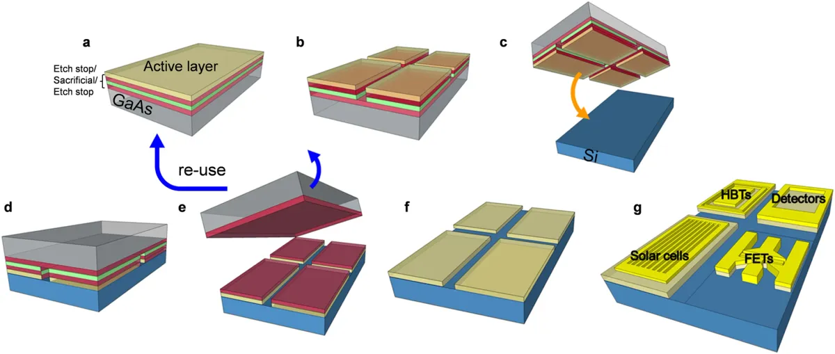
Key technical challenges include high costs versus silicon, driven by complex growth, lower yields, and smaller wafer sizes (mainstream 4- and 6-inch; 150 mm is the current commercial maximum). GaAs is brittle, prone to bowing and dislocations in larger formats, and arsenic handling adds toxicity and waste-management burdens. Emerging solutions focus on reclaim/recycling of epi-ready wafers, process optimizations for higher throughput /Scientific Reports/, defect reduction, and R&D into remote epitaxy /MRS Communications/ or improved VGF techniques that could cut material use, waste, and per-die costs over time.
The GaAs wafer market stands at roughly $1.4 billion in 2026 and is forecast to grow at 10–13% CAGR through the early 2030s, propelled by 5G infrastructure, exploding AI optical interconnect needs (VCSELs for 400G/800G+ links), defense electronics, and space photovoltaics /Mordor Intelligence/. RF remains the largest segment today, but optoelectronics and photonics are the fastest-growing as AI clusters demand ever-higher bandwidth density and energy efficiency.
Supply is highly concentrated and geopolitically sensitive. Global primary low-purity gallium production is ~760 tonnes annually, with China controlling ~99%. The leading substrate producers like Sumitomo Electric (Japan, ~29% share), Freiberger Compound Materials (Germany, ~21%), and AXT Inc. (US-listed with major China operations, ~15%) dominate the market. Recycling potential from GaAs manufacturing scrap and end-of-life devices is substantial but currently under-realized (new scrap recovery historically ~27%, old scrap <1%). Western nations lack meaningful gallium stockpiles and face export-control risks /CSIS/; diversification, domestic refining of scrap into high-purity material, and allied capacity expansion are now strategic priorities to secure resilient supply for AI and national security applications. Innovation in cost-effective, larger-scale, and circular GaAs production will determine how quickly and securely the AI ecosystem can scale its most demanding RF and photonic layers.
Key Insights
What are the estimated volumes of GaAs-based components (such as VCSELs on GaAs substrates) in NVIDIA’s Vera Rubin AI accelerator architecture and rack-scale systems?
GPU-to-optical-module ratios are rising to 4–6 in the Vera Rubin era, up from 2–3 in prior generations, with optical component TAM expanding nearly 10x by Rubin Ultra scale. Because many short-reach AI interconnects rely on GaAs VCSEL arrays, this drives dozens of GaAs dies per GPU and thousands per rack-scale NVL system. The surge directly amplifies demand for GaAs substrates in high-bandwidth, low-power optical links essential to next-generation AI clusters.
What is the most critical bottleneck process technology in GaAs substrate manufacturing for AI optoelectronics and RF applications?
The core bottleneck is single-crystal growth via LEC or VGF methods, which must achieve ultra-low defect densities and 6N+ purity while contending with GaAs brittleness. Commercial production remains limited to 4- and 6-inch wafers (far behind silicon) restricting economies of scale, raising costs, and hindering high-volume epitaxy for AI VCSELs. Arsenic handling and yield losses compound the challenge; reclaim and diameter-scaling R&D are advancing but have not yet resolved the fundamental limits on cost and supply elasticity.
What are the main supply chain and geopolitical risks for GaAs substrates amid rising AI data center demand in 2026?
China controls ~99% of primary gallium production, creating acute concentration risk amplified by tightened export controls since 2025. The substrate market is dominated by Sumitomo Electric, Freiberger, and AXT (with major China operations), while recycling rates stay low. These factors threaten timely scaling of GaAs VCSELs and RF components critical for AI optical interconnects, even as Western diversification and new capacity efforts accelerate but continue to lag AI-driven demand growth.