Tungsten Vias & Contacts: The Critical Mineral Powering AI Chip Interconnects
- David Rogers
- AI Buildout Supply Chain
- 2026-06-25
NEED TO KNOW
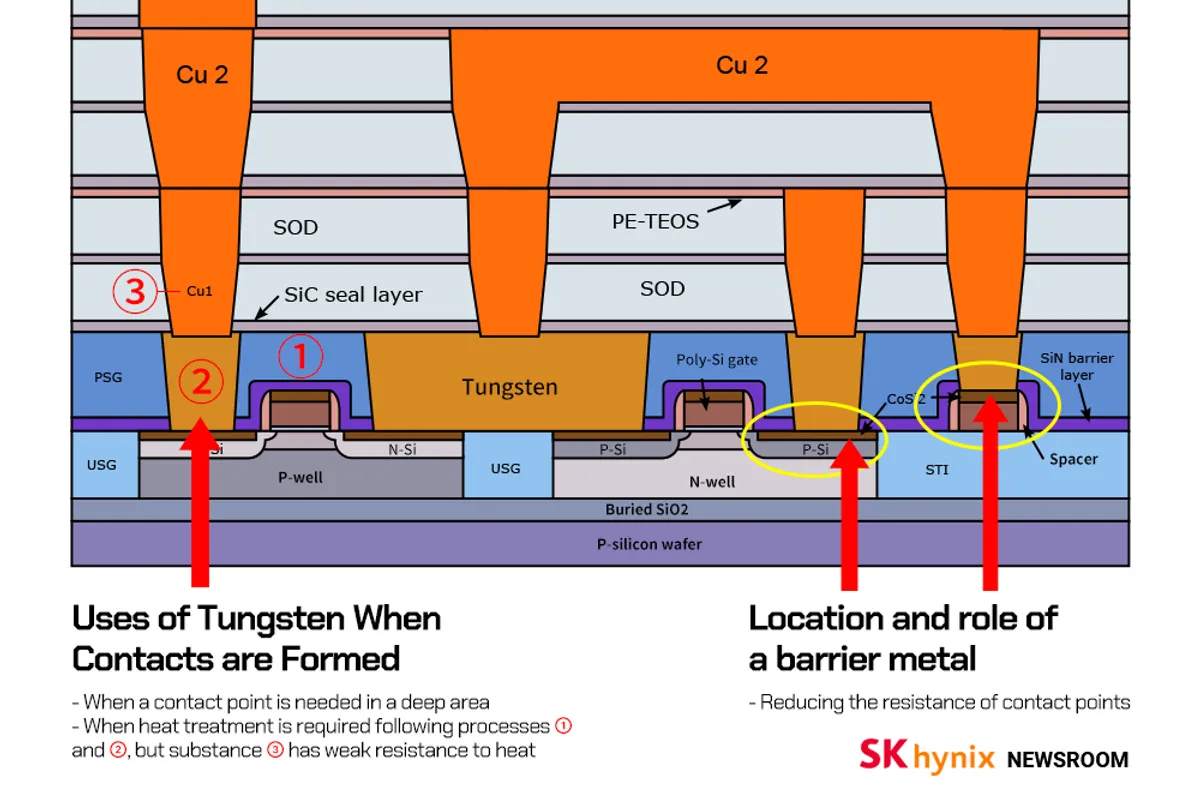
- Foundational Transistor Contact: Tungsten (WF₆ CVD deposition) forms non-replaceable contact plugs and high-aspect-ratio vias connecting transistors to metal interconnects in sub-7nm logic, HBM stacks, and 3D NAND.
- China Monopolizes ~80% of Supply: China controls ~80% of global tungsten mining and refining, while the US has had no active commercial tungsten mining since 2015, leaving Western fabs vulnerable to export licensing.
- Ultra-High Purity Requirements: Semiconductor-grade WF₆ gas requires 6N+ (99.9999%) purity with parts-per-billion metallic control to prevent voiding, beta-phase formation, and resistivity spikes.
- Western Diversification Initiatives: Projects like Almonty’s Sangdong mine in South Korea and domestic chemical recycling (e.g., Buffalo Tungsten) aim to supply up to 40% of non-Chinese demand.
Tungsten quietly anchors the most advanced AI chips. In leading-edge logic, HBM stacks, and 3D NAND, it forms the critical contacts that link transistors to the interconnect network and fills the high-aspect-ratio vias that route signals between layers. Its combination of low resistivity, superb step coverage via tungsten hexafluoride (WF6), a volatile gas that acts as a precursor in chemical vapor deposition (CVD) processes /China Isotope/, thermal stability, and resistance to electromigration makes it indispensable for reliable performance as nodes shrink below 7–10 nm and chips stack higher under extreme thermal and electrical stress. No near-term material fully replaces it for these conformal, high-reliability fills.
Producing semiconductor-grade tungsten demands exceptional purity and control. Ore (primarily scheelite or wolframite) is beneficiated to 65%+ WO₃ concentrate /MSR/, chemically processed through alkaline or acid leaching and purification to ammonium paratungstate (APT), then reduced to ultra-high-purity tungsten powder. This powder reacts with fluorine to yield WF6 gas, which is distilled to >99.999% (often 6N+) purity with parts-per-billion metallic impurities before CVD deposition of tungsten plugs and thin films. The unique capability lies in enabling dense, void-free fills in shrinking features where copper struggles thereby directly enabling the density and reliability gains AI accelerators require.
Technical and cost challenges are intensifying. Maintaining parts-per-billion level purity at commercial scale is difficult; impurities trigger defects, higher resistivity, or beta-tungsten phases. Traditional refining is energy-intensive, corrosive, and generates high-salinity wastewater. Emerging solutions include yield-boosting ore processing advances (claimed 7–12% improvements) /ScienceDirect/, chemical recycling back to ammonium paratungstate (APT), and early-stage bioleaching from semiconductor waste, though the latter remains costly and pre-commercial for ultra-pure grades. New primary capacity takes 5–10+ years to develop and qualify for fabs, while recycling already supplies roughly 30% of global tungsten but faces purity hurdles for semiconductor reuse.
AI-driven demand is structurally lifting the market. Hyperscale data centers, AI training clusters, and advanced packaging, including through-silicon vias (TSVs), require more chips with denser, more robust interconnects. The semiconductor industry is on track for explosive growth toward the $1 trillion mark, with AI infrastructure as the primary accelerator. Along the way, semiconductor fabrication processes are changing through the increasing adoption of hybrid metallization schemes, where alternative metals replace tungsten or copper in upper interconnect layers, combined with the explosive growth of 3D stacking, TSVs, and higher via/contact densities per chip enabled by advanced patterning, which together can sustain or even raise overall tungsten demand specifically for contact and via fills. Tungsten prices (concentrate and APT) surged sharply in 2025 amid this demand wave plus supply constraints, underscoring its role as a foundational enabler rather than a niche material.
Supply concentration creates acute geopolitical risk. China controls roughly 80% of global tungsten production and refining, with recent export licensing and U.S. tariffs amplifying price volatility and allocation uncertainty with Japan seeing imports drop ~50% in one recent month /Nikkei/. Tungsten world reserves exceed 4.7 million tonnes (China ~2.5 Mt, Vietnam surprisingly large at ~1.7 Mt), yet midstream processing outside China lags. The U.S. has had no commercial mining since 2015 and remains heavily import-dependent. Positive developments include Almonty’s Sangdong mine in South Korea (Phase 1 now producing ~2,300 t concentrate/year, targeting ~40% of non-Chinese demand at full capacity) and Western recycling/powder efforts (e.g., Buffalo Tungsten supplying WF6 feedstock, Japanese/Korean WF6 producers, and equipment leaders like Applied Materials and Lam Research).
Building resilient tungsten supply chains for the AI era will require parallel progress: accelerated non-Chinese mining and powder/WF6 qualification, scaled high-purity recycling, and allied coordination. Without it, the physical backbone of AI intelligence remains vulnerable to disruption.
Key Insights
What is the function of tungsten in advanced AI semiconductor chips?
Tungsten forms the contact plugs and high-aspect-ratio vias that connect transistors to the metal interconnect layers in logic chips, high-bandwidth memory, and 3D NAND stacks. Deposited via chemical vapor deposition using tungsten hexafluoride gas, tungsten offers low resistivity, excellent step coverage, and high resistance to electromigration, making it indispensable for chips scaled below 10 nanometers.
How dominant is China in the global tungsten supply chain, and what are the risks?
China controls approximately 80% of global tungsten mining and refining, exposing international chipmakers to export licensing restrictions and supply disruptions. While global reserves exceed 4.7 million tonnes, the United States has had no commercial tungsten mining since 2015, leaving the Western semiconductor manufacturing industry heavily reliant on imported materials.
What projects are being developed to diversify the supply of tungsten for chipmakers?
Almonty Industries is ramping up production at the Sangdong mine in South Korea, targeting 2,300 tonnes of concentrate annually to supply roughly 40% of non-Chinese demand. Additionally, Western companies like Buffalo Tungsten are expanding chemical recycling and powder processing to generate secure domestic feedstocks for tungsten hexafluoride gas production.